Silicon carbide semiconductor device and method for producing the same

Active Publication Date: 2015-05-14
DENSO CORP +1
View PDF1 Cites 27 Cited by
  • Summary
  • Abstract
  • Description
  • Claims
  • Application Information

AI Technical Summary

Benefits of technology

[0015]As described above, the second conductivity type layer is made of the bottom layer located at the bottom portion of the trench and the end layers formed at both of the ends of the trench, so that the bottom layer is connected to the base region through the end layers. In the SiC semiconductor device having such a structure, when the semiconductor switching element is turned off, an electric field hardly enter due to a depletion layer extending from the bottom layer to

Problems solved by technology

Therefore, a producing process is likely to be complex, for example, due to transferring the work to an ion-implantation apparatus, resulting in the increase in manufacturing costs.
F

Method used


Image

  • Silicon carbide semiconductor device and method for producing the same
  • Silicon carbide semiconductor device and method for producing the same
  • Silicon carbide semiconductor device and method for producing the same

Examples


first embodiment

[0030]A first embodiment of the present disclosure will be described. In this case, an SiC semiconductor device formed with an n-channel inversion type MOSFET as a semiconductor switching element with a trench gate structure will be described as an example.

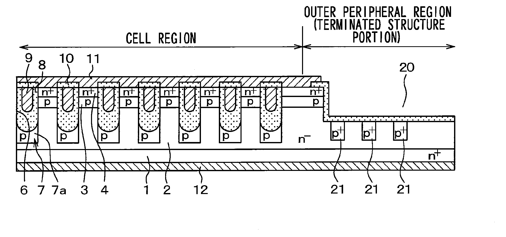
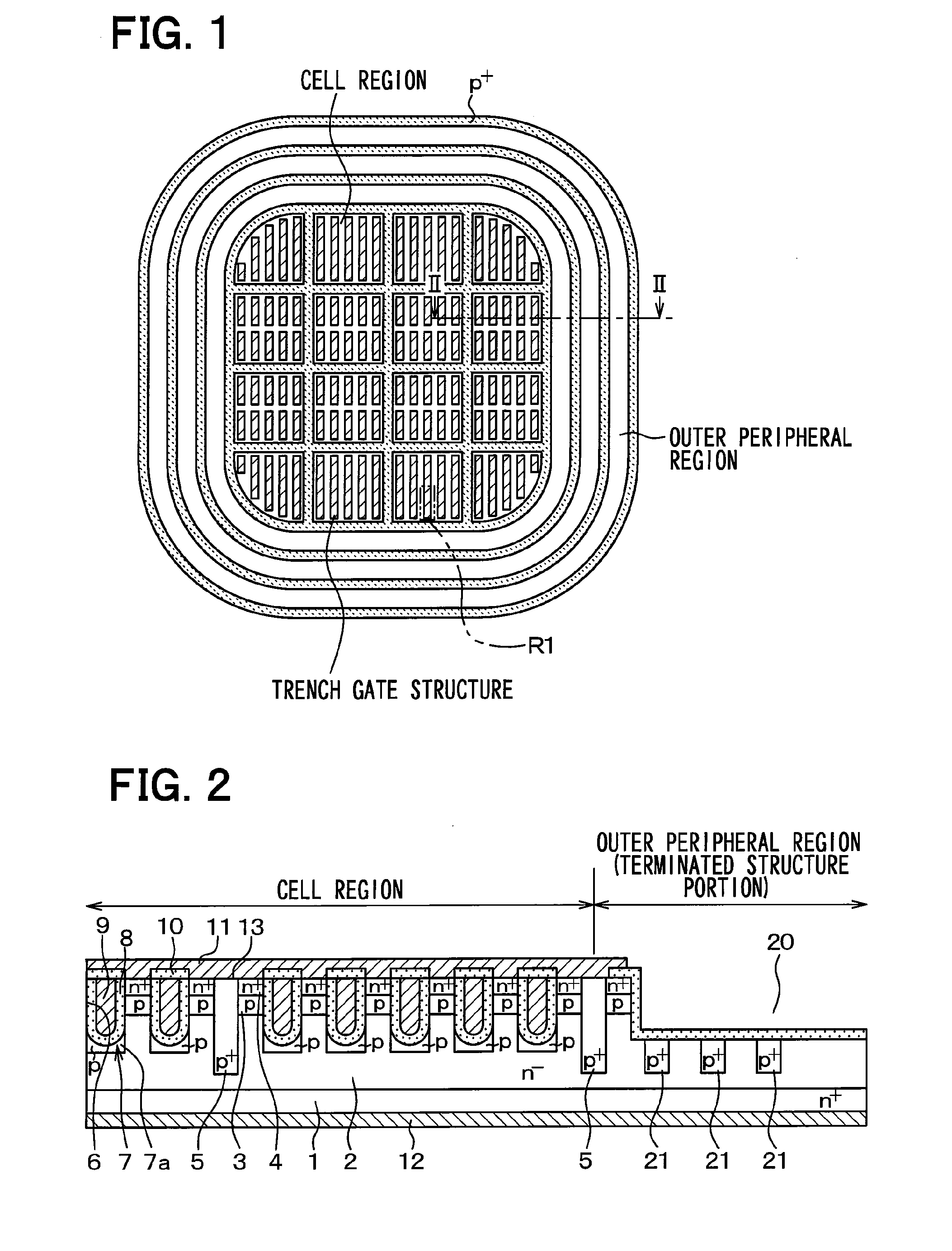
[0031]An SiC semiconductor device shown in FIG. 1 has a cell region formed with a semiconductor element and an outer peripheral region (terminated structure region) provided with an outer peripheral withstand voltage structure surrounding the cell region. In the present embodiment, the SiC semiconductor device has the MOSFET with an inversion type trench gate structure as the semiconductor element.

[0032]As shown in FIG. 2, the SiC semiconductor device employs a semiconductor substrate in which an n− type drift layer 2, a p type base region 3, and an n+ type source region 4, which are made of SiC, are epitaxially grown on a main surface of an n+ type substrate 1 made of SiC.

[0033]The n+ type substrate 1 is, for example, 1.0×10¹⁹ / c...

second embodiment

[0070]A second embodiment of the present disclosure will be described. In the present embodiment, the structure of the p+ type deep layer 5 is modified from that of the first embodiment. The others are similar to the first embodiment, and thus only the part different from the first embodiment will be described.

[0071]The SiC semiconductor device shown in FIG. 7 also includes the cell region in which a semiconductor element is formed and the outer peripheral region. However, the layout of the p+ type deep layer 5 formed in the cell region is different from that of the first embodiment. Specifically, as shown in the enlarged view of FIG. 8, the trench gate structure is divided into plural sections in the longitudinal direction, and the p+ type deep layer 5 is arranged to overlap the end portion of each of the divided trench gate structures. The p+ type deep layer 5 is formed into a line shape to continuously intersect with the divided trench gate structures that are arranged in paralle...

third embodiment

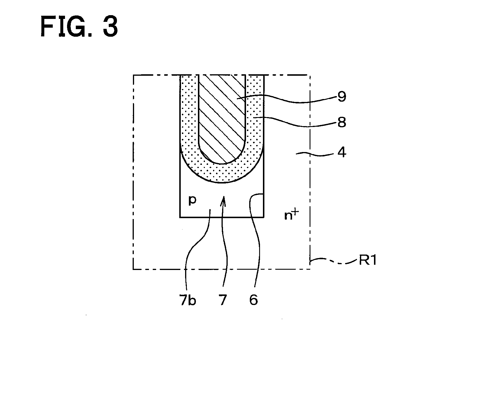
[0075]A third embodiment of the present disclosure will be described. In the present embodiment, the p+ type deep layer 5 is eliminated from the structure of the first embodiment, and the structure of the trench gate structure is modified from that of the first embodiment. The others are similar to those of the first embodiment. Therefore, only the parts different from the first embodiment will be described.

[0076]The SiC semiconductor device shown in FIG. 11 also includes the cell region in which the semiconductor element is formed and the outer peripheral region. However, the p+ type deep layer 5 is not formed in the cell region. In the trench gate structure of the present embodiment, as shown in FIG. 12, the depth of the trench 6 is increased, and, at the bottom portion and the end portions of the trench 6, the p type SiC layer 7 (the bottom p type layer 7a and the end p type layers 7) is formed and the thickness of the gate insulation film 8 is increased. The upper surface of a r...


PUM


Abstract

In a method for producing an SiC semiconductor device, a p type layer is formed in a trench by epitaxially growing, and is then left only on a bottom portion and ends of the trench by hydrogen etching, thereby to form a p type SiC layer. Thus, the p type SiC layer can be formed without depending on diagonal ion implantation. Since it is not necessary to separately perform the diagonal ion implantation, it is less likely that a production process will be complicated due to transferring into an ion implantation apparatus, and thus manufacturing costs reduce. Since there is no damage due to a defect caused by the ion implantation, it is possible to reduce a drain leakage and to reliably restrict the p type SiC layer from remaining on the side surface of the trench.

Description

CROSS REFERENCE TO RELATED APPLICATIONS[0001]This application is based on Japanese Patent Application No. 2012-134917 filed on Jun. 14, 2012, the disclosure of which is incorporated herein by reference.TECHNICAL FIELD[0002]The present disclosure relates to a silicon carbide (hereinafter referred to as SiC) semiconductor device having a semiconductor switching element with a trench gate structure, and a method for producing the same.BACKGROUND ART[0003]In a semiconductor device having a semiconductor switching device, an increase in channel density is effective to allow a larger current to flow. In a silicon transistor, a MOSFET with a trench gate structure is employed so as to increase the channel density, and such a silicon transistor has been put into practice. Although the trench gate structure can be employed to an SiC semiconductor device, the SiC has a breakdown electric field intensity of ten times as high as that of silicon. Therefore, the SiC semiconductor device is used in...

Claims


Application Information

Patent Timeline
IPC IPC(8): H01L29/66H01L29/423H01L29/78H01L21/04H01L29/16
CPCH01L29/66068H01L21/0455H01L29/4236H01L29/1608H01L29/7827H01L21/049H01L29/045H01L29/0619H01L29/0623H01L29/0661H01L29/0696H01L29/1095H01L29/7397H01L29/7811H01L29/7813H01L21/3065H01L21/02529H01L21/0475H01L29/66348H01L29/66734
Inventor TAKEUCHI, YUICHICHIDA, KAZUMISOEJIMA, NARUMASAWATANABE, YUKIHIKO
Owner DENSO CORP
Why Eureka
Try Eureka