

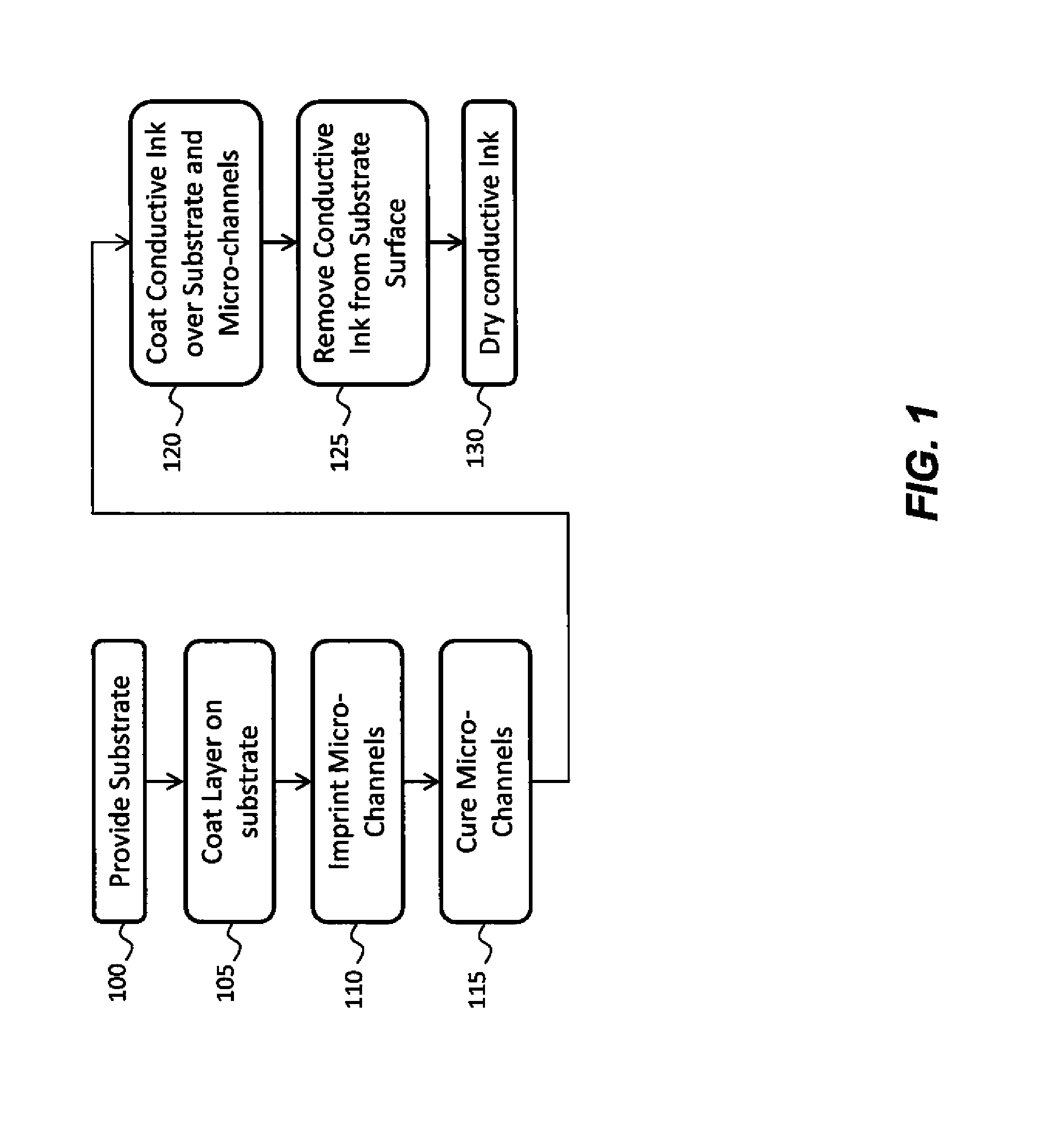
Preparation of articles with conductive micro-wire pattern
a micro-wire pattern and pattern technology, applied in the field of micro-wire pattern formation, can solve the problems of reducing the conductivity of micro-wires, unable to readily form dispersions into conductive compositions, and limited electric conductivity generated by such conductive compositions
- Summary
- Abstract
- Description
- Claims
- Application Information
AI Technical Summary
Benefits of technology
Problems solved by technology
Method used
Image

Examples
example 1
[0148]A poly(ethylene terephthalate) film having a dry thickness of about 125 μm that had been surface coated with a poly(vinylidene chloride) containing latex to form an adhesion promotion subbing layer was used as a substrate. The coating formulation shown below in TABLE I was applied as photocurable compositions over the adhesion promotion subbing layer and dried to form photocurable layers for each precursor article, each photocurable layer having a dry thickness of about 5.5 μm.
TABLE IMaterialWeight %Epon SU-8 (Momentive34Performance Materials)Coatosil MP-2006Triarylsulfonium4.8hexafluorophosphatemixed salts (50% inpropylene carbonate)photoinitiatorMethyl ethyl ketone55.2(MEK)
[0149]The viscosity and elastic modulus of each photocurable composition was measured without the presence of a photoinitiator for easy handling. The viscosity was about 65 Pascal-seconds at 60° C. and 3333 Pascal-seconds at 40° C., and the elastic modulus was about 3 Pascals at 60° C. and 1111 Pascals at ...
example 2
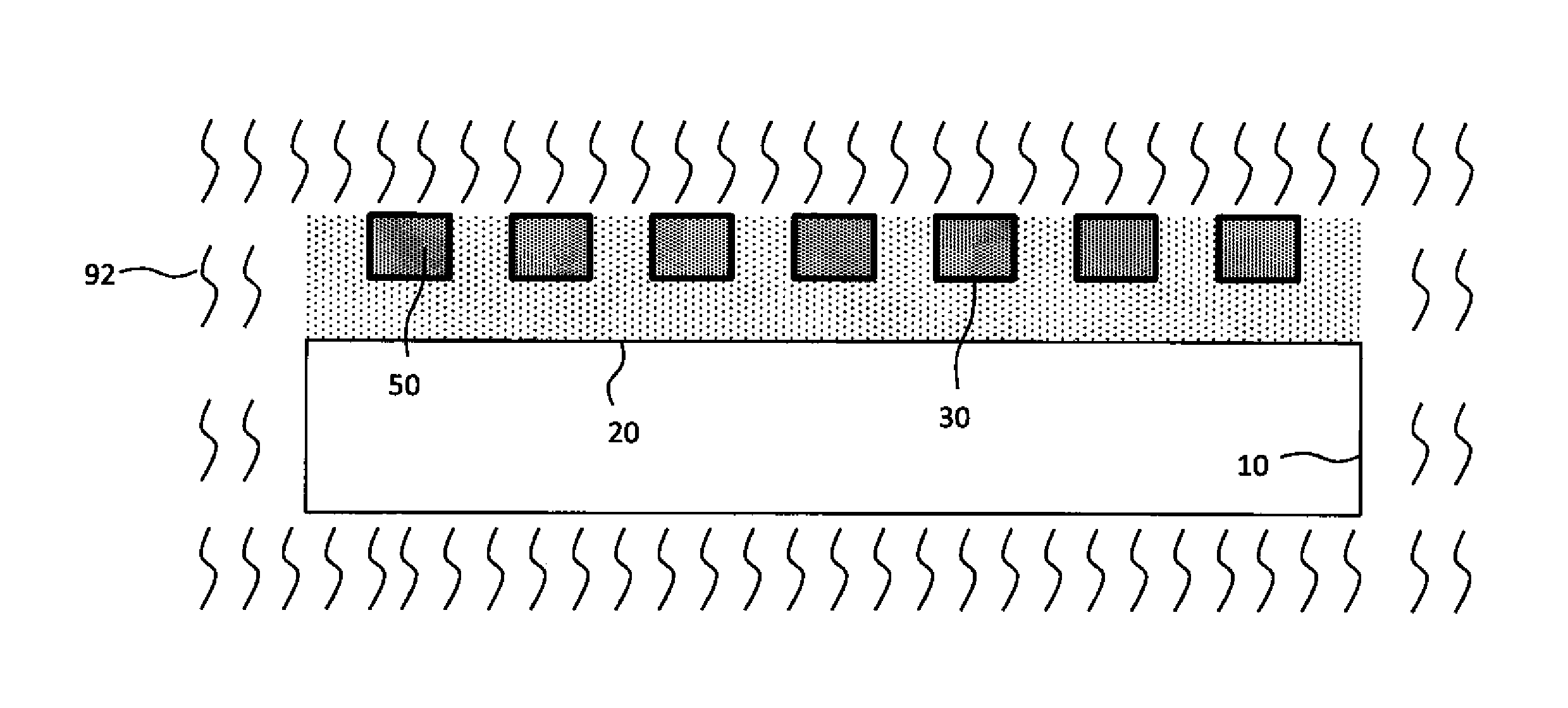
[0155]A photocurable composition having a 85 / 15 weight ratio of Epon SU-8 to Coatosil MP-200 was used to form a dry photocurable layer having a dry thickness of about 7 μM over a transparent poly(ethylene terephthalate) film substrate. The dry photocurable layer was then pressed against a transparent elastomeric mold made from Dow Corning Sylgard 184 siloxane elastomer at 70° C. for about 3 minutes at 5 psi (0.034 MPa) and 2 minutes at 25 psi (0.17 MPa) followed by exposure to ultraviolet light to cure the dry photocurable layer to form a pattern of photocured micro-channels. The transparent elastomeric mold had a test structure containing separate lines at various widths from 2 to 20 μm and each line having an average height of about 4 μm and a length of about 10 mm.
[0156]After the UV light exposure, the elastomeric mold was separated from the dry photocured layer having micro-channels exhibiting the testing structure described above except that the testing structure had separate m...
PUM
| Property | Measurement | Unit |
|---|---|---|
| distortion temperature | aaaaa | aaaaa |
| width | aaaaa | aaaaa |
| width | aaaaa | aaaaa |
Abstract
Description
Claims
Application Information