System and method for forming gan-based device

Inactive Publication Date: 2015-07-02
ENKRIS SEMICON
View PDF7 Cites 0 Cited by
  • Summary
  • Abstract
  • Description
  • Claims
  • Application Information

AI Technical Summary

Benefits of technology

This patent presents a vacuum interconnecting system that is used to transfer silicon substrates between different reaction chambers for the formation of thin films and epitaxial layers. By using this system, the substrates are not exposed to air, which improves the quality of the thin films formed and reduces surface oxidation. The system also includes a cleaning chamber for cleaning the substrates and reducing current collapse. The process of forming nitride layers and dielectric films in the same system reduces cross contamination and surface oxidation, leading to improved device performance. The system can also be used to repeatedly form nitride films without the need for cleaning. Overall, this patent provides a more efficient and high-quality method for the formation of thin films and epitaxial layers in semiconductor devices.

Problems solved by technology

Thus, GaN based power switches may have very low on-state resistance under the same breakdown voltage.
Compared with GaN based light emitting devices, GaN power switching devices are more sensitive to production cost.
As a result, compared with Si based devices, GaN based devices are required to have better performance, and also competitive costs.
However, it is very difficult to grow GaN on a Si substrate.
Due to the large lattice mismatch and thermal mismatch between Si and GaN, GaN epi-layers grown Si in general show large wafer bow or even cracks without stress engineering.
In addition, Ga atoms may act with Si atoms and result in melt back etching effect.

Method used


Image

  • System and method for forming gan-based device
  • System and method for forming gan-based device
  • System and method for forming gan-based device

Examples


Embodiment Construction

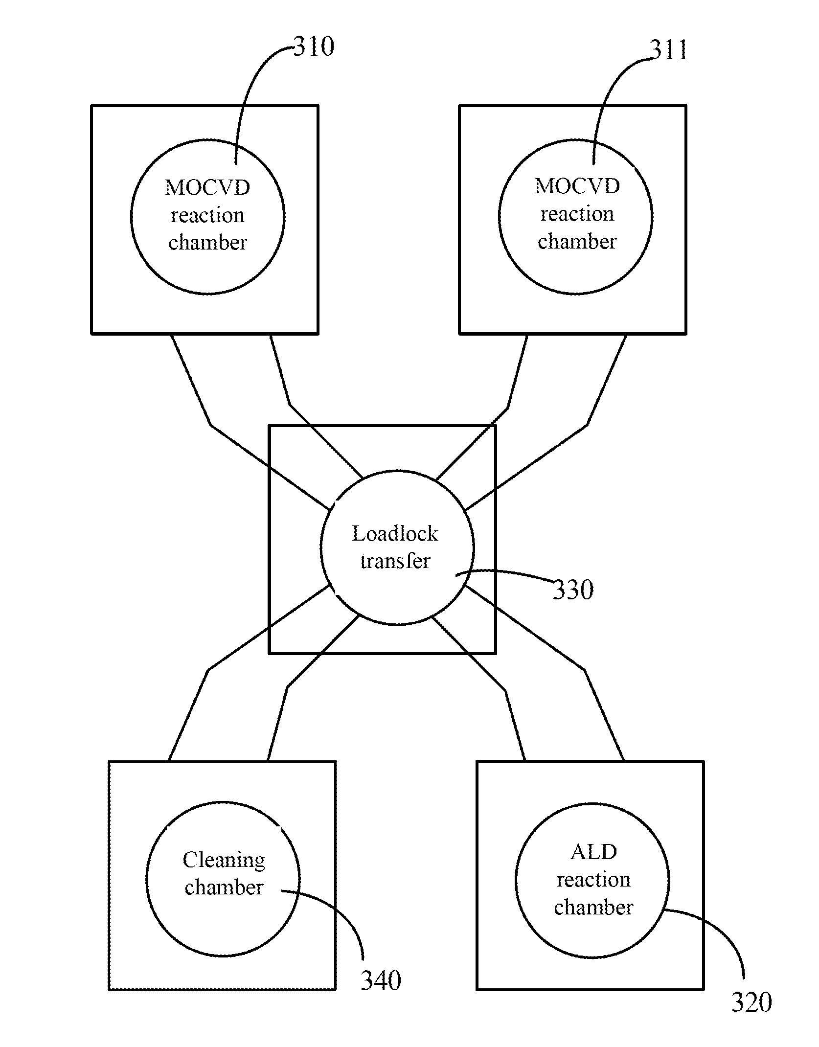
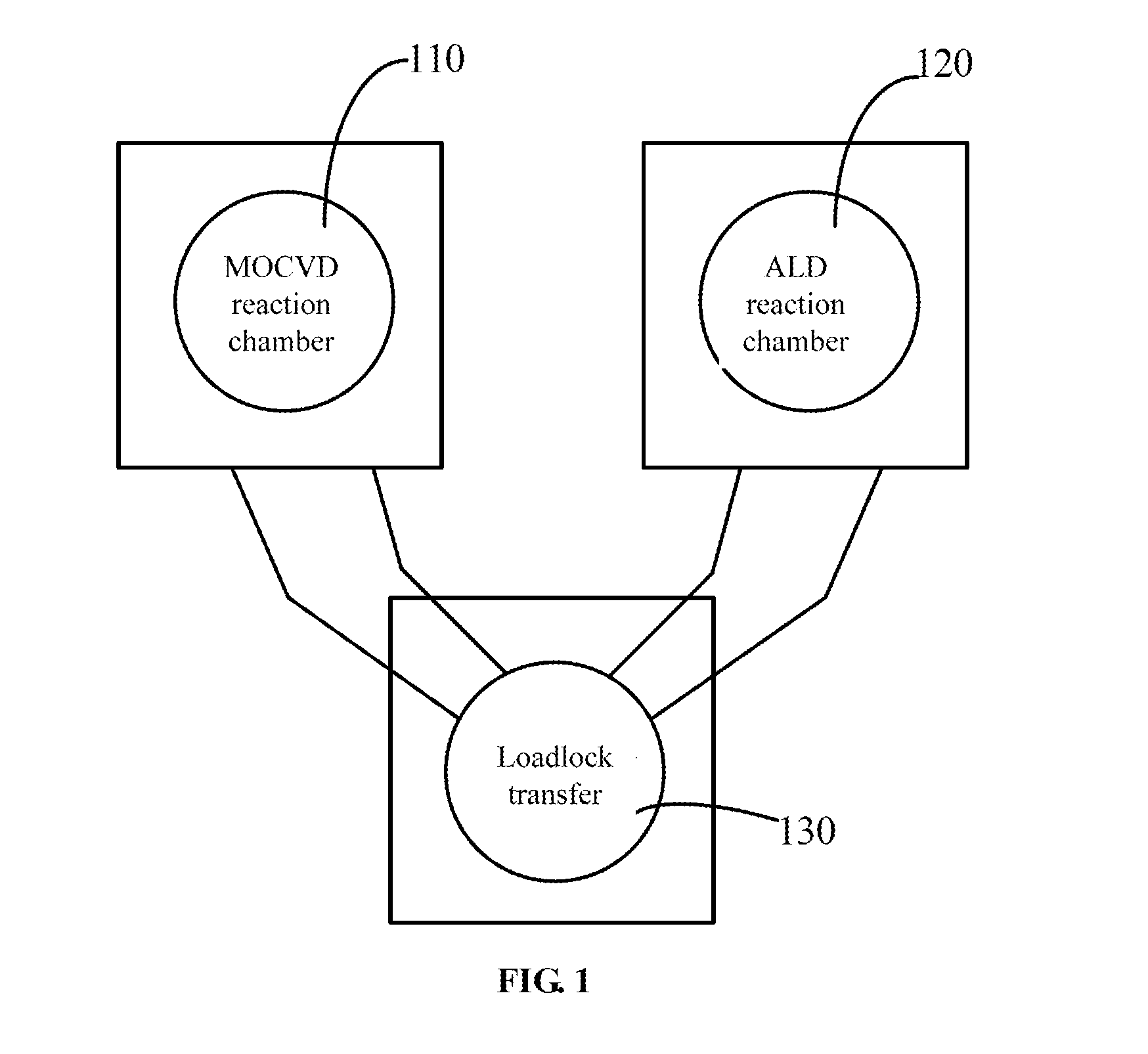
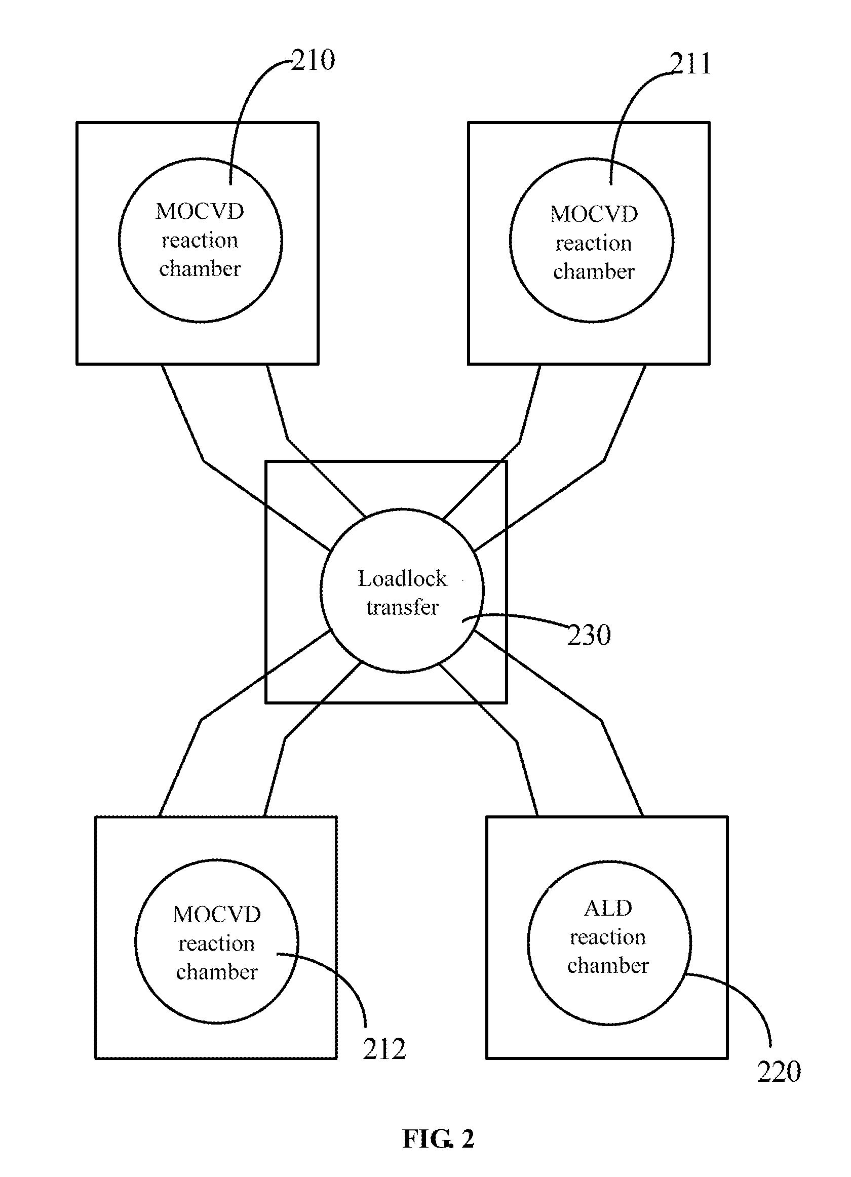
[0045]Embodiments of the present disclosure provide a system for forming a GaN based device. The system is an integrated system which includes:[0046]at least one metal organic chemical vapor deposition (MOCVD) reaction chamber;[0047]at least one atomic layer deposition (ALD) reaction chamber or chemical vapor deposition (CVD) reaction chamber; and[0048]a loadlock transfer connecting with the at least one MOCVD reaction chamber and the at least one ALD reaction chamber.

[0049]Accordingly, embodiments of the present disclosure provide a method for forming a GaN based device, including:[0050]providing a plurality of reaction chambers including at least one MOCVD reaction chamber and at least one ALD reaction chamber;[0051]using a loadlock transfer to feed a device to be processed to the plurality of reaction chambers for implementing corresponding processes according to a predetermined sequence, where each of the plurality of reaction chambers supplies corresponding gas or liquid or pla...


PUM

PropertyMeasurementUnit
Temperatureaaaaaaaaaa

Abstract

A system and a method for forming a GaN based device are provided. The system may include: at least one MOCVD reaction chamber; at least one ALD or CVD reaction chamber; and a loadlock transfer connecting with the MOCVD reaction chamber and the ALD or CVD reaction chamber. The MOCVD reaction chamber may be a standard chamber for nitride growth. The ALD or CVD reaction chamber may be used for growing nitride and oxide dielectric layers, which may have a highest growth temperature no less than about 500° C., such that nitride and oxide may have better qualities. The system may include a cleaning chamber for cleaning the substrate and the nitride films. Using the integrated system, cleaning processes and growing processes for epitaxial layers and dielectric layers can be implemented in a same system, which may avoid contaminations in the air. Device performance may be improved.

Description

FIELD OF THE DISCLOSURE[0001]The present disclosure generally relates to micro electric technology, and more particularly, to a system and a method for forming a GaN-based device.BACKGROUND OF THE DISCLOSURE[0002]GaN is identified as the most important semiconductor material after Si. GaN is a wide band gap material, and its spectrum covers the whole visible light region. GaN can be used to form following optical devices: blue and white light emitting diodes (LEDs) for illustration, TV backlight and general illumination; green and blue LEDs for full color display together with AlGaInP based red LEDs; and ultra-violet (UV) laser diodes for data storage. In addition to its outstanding optical characteristics, GaN also has remarkable electrical properties, such as high electron mobility (about 2000 cm2 / VS in 2DEG), high electron saturated drift velocity (about 2.5E7 cm / s), high critical electrical field (about 3.5 MV / cm), and etc. GaN can also be used in RF and power electronics applic...

Claims


Application Information

Patent Timeline
IPC IPC(8): H01L21/67C23C16/458C23C16/34C23C16/50
CPCH01L21/67201H01L21/67167C23C16/34C23C16/50C23C16/458H01L21/67207C30B25/02C30B29/406
Inventor CHENG, KAI
Owner ENKRIS SEMICON
Why Eureka
Try Eureka