SiC Single-Crystal Ingot, SiC Single Crystal, and Production Method for Same
a single crystal, sic single crystal technology, applied in the direction of crystal growth process, polycrystalline material growth, water-setting substance layered product, etc., can solve the problems of polymorphic crystal generation, lattice defects, hollow penetration defects of grown single crystals, etc., to achieve low threading and low resistivity
- Summary
- Abstract
- Description
- Claims
- Application Information
AI Technical Summary
Benefits of technology
Problems solved by technology
Method used
Image
Examples
example 1
[0079]There was prepared a SiC single crystal formed by a sublimation process, which was a discoid 4H—SiC single crystal with a diameter of 12 mm, a thickness of 700 μm, and the bottom face as the (0001) plane, for use as a seed crystal substrate. The seed crystal substrate had a threading dislocation density of 7×10³ / cm2, a resistivity of 20 mQ·cm and a nitrogen density of 1×10¹⁹ / cm3. The top face of the seed crystal substrate was bonded to roughly the center section of the end face of a cylindrical graphite shaft, using a graphite adhesive.
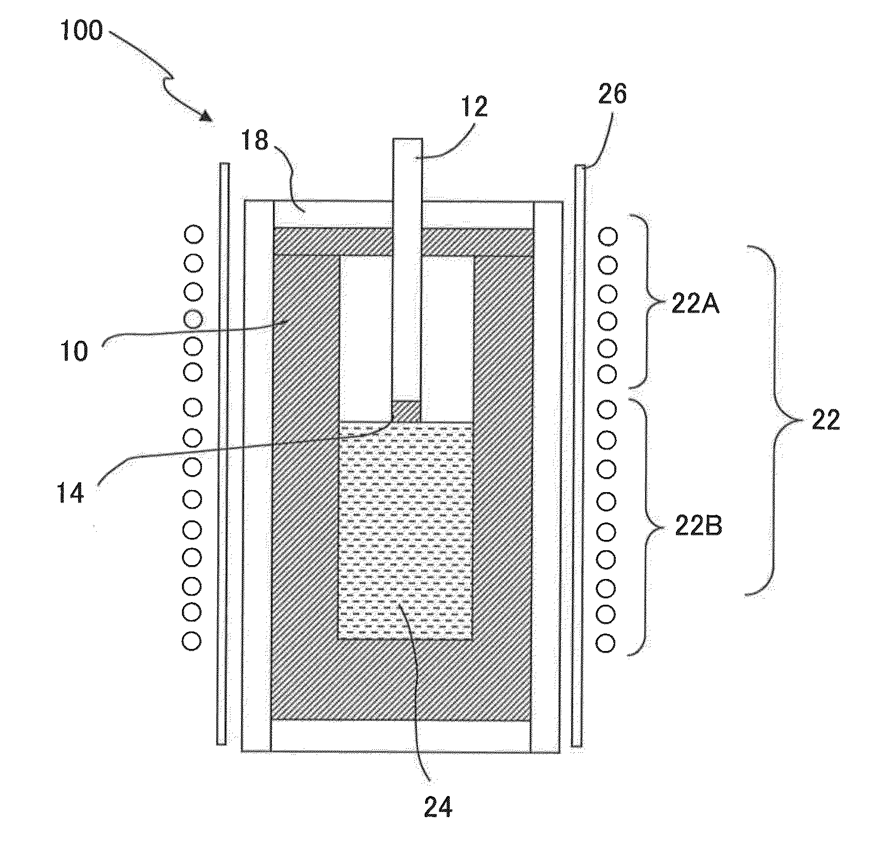
[0080]A single crystal production apparatus as shown in FIG. 1 was used, and Si / Cr / Ni was loaded as a molten liquid starting material into a graphite crucible for housing a Si—C solution. Vacuum suction of the interior of the single crystal production apparatus was performed down to 1×10⁻³ Pa and argon gas was then introduced into the single crystal production apparatus up to 91 kPa so that the air inside the single crystal production apparatus ...
example 2
[0087]A crystal was grown and recovered under the same conditions as Example 1, except that an argon partial pressure and a nitrogen partial pressure before seed touching were controlled to 91 kPa and 2 kPa, respectively. The threading dislocation density, resistivity and nitrogen density of the grown crystal were then measured under the same conditions as Example 1.
[0088]The obtained grown crystal was a SiC single crystal having a diameter of 12 mm and a thickness of 1 mm, of which the nitrogen density gradient layer constituted a thickness of 30 μm and the nitrogen density constant layer constituted a thickness of 0.97 mm. The threading dislocation density of the nitrogen density constant layer was 7×10³ / cm2, and the resistivity was 6 mΩ·cm. The nitrogen density of the nitrogen density constant layer was 6×10¹⁹ / cm3, and the rate of change of the nitrogen density of the nitrogen density gradient layer was 6000% / mm. No micropipe defects were present in the grown crystal.
example 3
[0089]A crystal was grown and recovered under the same conditions as Example 1, except that an argon partial pressure and a nitrogen partial pressure before seed touching were controlled to 91 kPa and 5 kPa, respectively. The threading dislocation density, resistivity and nitrogen density of the grown crystal were then measured under the same conditions as Example 1.
[0090]The obtained grown crystal was a SiC single crystal having a diameter of 12 mm and a thickness of 1 mm, of which the nitrogen density gradient layer constituted a thickness of 30 m and the nitrogen density constant layer constituted a thickness of 0.97 mm. The threading dislocation density of the nitrogen density constant layer was 7×10³ / cm2, and the resistivity was 6 mΩ·cm. The nitrogen density of the nitrogen density constant layer was 6×10¹⁹ / cm3, and the rate of change of the nitrogen density of the nitrogen density gradient layer was 3000% / mm. No micropipe defects were present in the grown crystal.
PUM
| Property | Measurement | Unit |
|---|---|---|
| resistivity | aaaaa | aaaaa |
| surface temperature | aaaaa | aaaaa |
| partial pressure | aaaaa | aaaaa |
Abstract
Description
Claims
Application Information


