Semiconductor device, or crystal

a semiconductor device and crystal technology, applied in the direction of crystal growth process, polycrystalline material growth, chemically reactive gases, etc., can solve the problems of difficult to form an insulating film of good quality, semiconductor devices have difficulty in having a normally-off device structure, and many problems to be solved, so as to reduce the cost of the substrate, simplify the device process steps, and improve the heat dissipation effect

Active Publication Date: 2015-07-09
FLOSFIA
View PDF13 Cites 20 Cited by
  • Summary
  • Abstract
  • Description
  • Claims
  • Application Information

AI Technical Summary

Benefits of technology

[0030]Since the above method uses, as a support substrate, a substrate which is not a corundum crystal, it is possible to use a substrate having a higher heat dissipation effect or to reduce the substrate cost. It is also possible to change the film formation order, for example, by forming an insulating film on a base substrate and then forming a semiconductor layer on the insulating film. Thus, it is possible to simplify the device process steps, such as ion implantation, etching, and photolithography,

Problems solved by technology

However, SiC and Ga semiconductor devices still have many problems to be solved.
A significant one of the problems is that these semiconductor devices have difficulty in having a normally-off device structure.
Particularly, for SiC-MOSFETs, this problem has been found to arise from the fact that it is difficult to form an insulating film of good quality in the MOS structure.

Method used


Image

  • Semiconductor device, or crystal
  • Semiconductor device, or crystal
  • Semiconductor device, or crystal

Examples


Embodiment Construction

[0041]Now, a preferred embodiment of a semiconductor device and a manufacturing method thereof according to the present invention will be described with reference to the accompanying drawings. Through the drawings, components having the same reference numerals are the same components.

[Method for Manufacturing Semiconductor Device, Corundum Crystal Film Forming Apparatus]

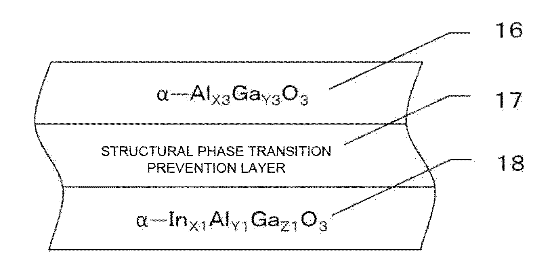
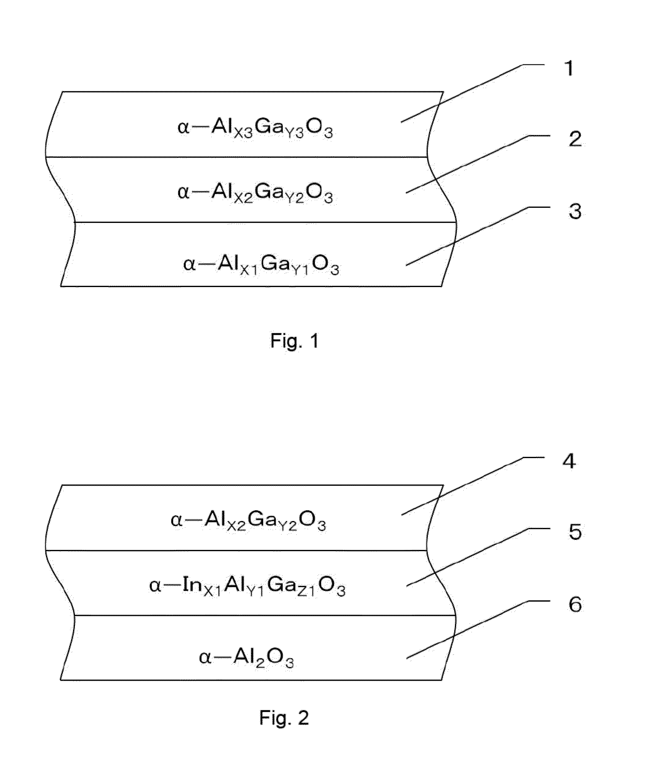
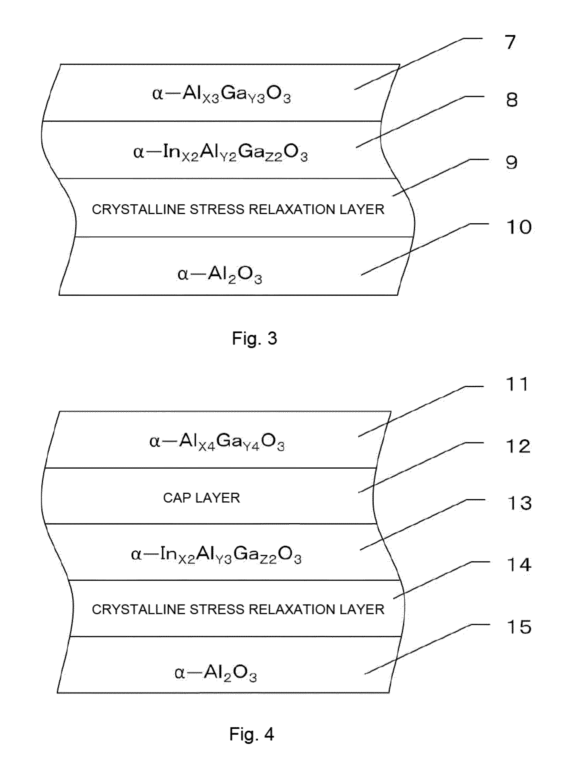
[0042]There will be described a method for manufacturing a semiconductor device and a film forming apparatus 10A used to form corundum crystal films.

[0043]A film forming apparatus 19 shown in FIG. 6 is a mist CVD apparatus and is configured as follows. That is, the film forming apparatus 19 includes a sample 20 on which films are to be formed, such as a base substrate, a sample stage 21, a nitrogen source 22, a flow rate control valve 23 for controlling the flow rate of nitrogen sent from the nitrogen source 22, a mist source 24 including a solution 24a, a container 25 containing water 25a, an ultrasonic transducer 2...


PUM

PropertyMeasurementUnit
temperatureaaaaaaaaaa
frequencyaaaaaaaaaa
temperatureaaaaaaaaaa

Abstract

There is provided a semiconductor device including corundum crystal films of good quality. There is provided a semiconductor device including a base substrate, a semiconductor layer, and an insulating film each having a corundum crystal structure. Materials having a corundum crystal structure include many types of oxide films capable of functioning as an insulating film. Since all the base substrate, the semiconductor layer, and the insulating film have a corundum crystal structure, it is possible to achieve a semiconductor layer and an insulating film of good quality on the base substrate.

Description

TECHNICAL FIELD[0001]The present invention relates to a semiconductor device or a crystal which is suitably used in power applications.BACKGROUND ART[0002]Promising next-generation switching devices capable of achieving high voltage, low loss, and high heat resistance include semiconductor devices which include silicon carbide (SiC) or gallium nitride (GaN), which has a large band gap. Such semiconductor devices are expected to be applied to power semiconductor devices, such as inverters.[0003]In particular, as with silicon, SiC-MOSFETs having a MOS structure on the substrate surface have been developed as SiC-based, high-voltage semiconductor devices.[0004]However, SiC and Ga semiconductor devices still have many problems to be solved. A significant one of the problems is that these semiconductor devices have difficulty in having a normally-off device structure.[0005]Particularly, for SiC-MOSFETs, this problem has been found to arise from the fact that it is difficult to form an in...

Claims


Application Information

Patent Timeline
Patent Type & Authority Applications(United States)
IPC IPC(8): H01L29/04H01L21/02H01L29/24
CPCH01L29/04H01L21/0262H01L21/02609H01L29/24C30B25/02C30B29/20C30B29/22H01L21/0237H01L21/0242H01L21/02488H01L21/02565H01L21/02628
Inventor KANEKO, KENTAROHITORA, TOSHIMIHIRAO, TAKASHI
Owner FLOSFIA
Why Eureka
Try Eureka