Solid-state image pickup unit and electronic apparatus

a solid-state image and electronic equipment technology, applied in the direction of thermoelectric devices, transistors, radiation controlled devices, etc., can solve the problems of difficult miniaturization of pixels, achieve the effect of reducing the smear noise generated by light entry, reducing the floating diffusion section, and reducing the smear nois

Active Publication Date: 2015-08-13
SONY SEMICON SOLUTIONS CORP
View PDF15 Cites 39 Cited by
  • Summary
  • Abstract
  • Description
  • Claims
  • Application Information

AI Technical Summary

Benefits of technology

[0034]Moreover, according to the configuration of the above-described solid-state image pickup unit of the embodiment of the present technology, the second charge accumulation section and the floating diffusion section are formed in the region other than the light-condensing region where incident light is condensed; therefore, an amount of light incident on the second charge accumulation section and the floating diffusion section is reduced. Accordingly, smear noise generated by entry of light is allowed to be reduced, thereby obtaining a high S / N ratio.
[0035]According to a configuration of the above-described electronic apparatus of the embodiment of the present technology, the solid-state image pickup unit of the present technology is included; therefore, in the solid-state image pickup unit, miniaturization of pixels is achieved, and simultaneous exposure in all pixels is possible; therefore, a high S / N ratio is obtained.
[0036]According to the solid-state image pickup unit of the embodiment of the present technology and the electronic apparatus including the solid-state image pickup unit, miniaturization of pixels is allowed to be achieved; therefore, downsizing and an increase in the number of pixels are allowed to be achieved. Then, a high-resolution image is allowed to be provided by achieving an increase in the number of pixels.
[0037]Moreover, simultaneous exposure in all pixels is possible; therefore, generation of distortion when an image of a moving subject is picked up is allowed to be prevented. Then, since simultaneous exposure in all pixels is possible without providing a light-shielding film, compared to a case where the light-shielding film is provided, an improvement in sensitivity and an improvement in a saturation charge amount are allowed to be achieved by expanding an opening.
[0038]Further, since smear noise is reduced to obtain a high S / N ratio, favorable image quality is allowed to be achieved.
[0039]Therefore, according to the solid-state image pickup unit of the embodiment of the present technology and the electronic apparatus including the solid-state image pickup unit, high sensitivity and a high saturation charge amount are allowed to be achieved, and an image with high resolution and favorable image quality is allowed to be provided.

Problems solved by technology

However, in a configuration in which the above-described photoelectric conversion film is provided, the first accumulation section and the second accumulation section are arranged along a lateral direction of the substrate; therefore, miniaturization of pixels is difficult.

Method used


Image

  • Solid-state image pickup unit and electronic apparatus
  • Solid-state image pickup unit and electronic apparatus
  • Solid-state image pickup unit and electronic apparatus

Examples


first embodiment (

1. First Embodiment (Solid-state image pickup unit)

2. First Modification Example of First Embodiment

3. Second Modification Example of First Embodiment

4. Third Modification Example of First Embodiment

5. Fourth Modification Example of First Embodiment

[0078]6. Second Embodiment (Solid-state image pickup unit)

7. Third Embodiment (Electronic apparatus)

1. First Embodiment

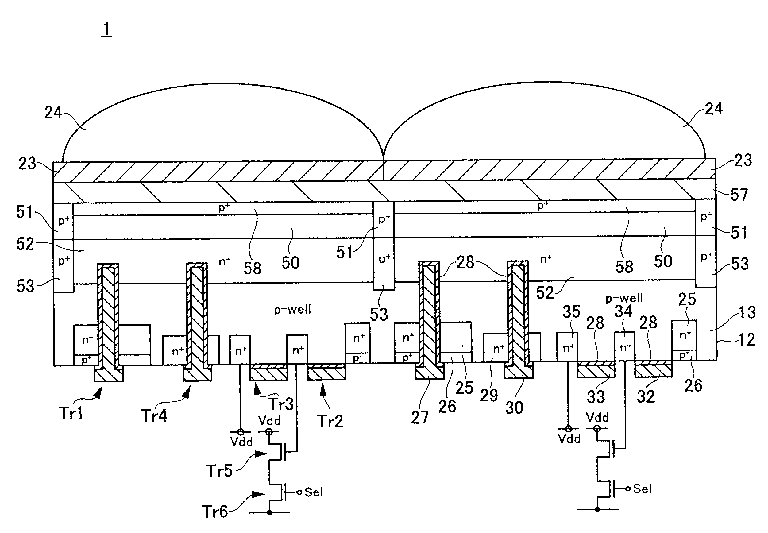
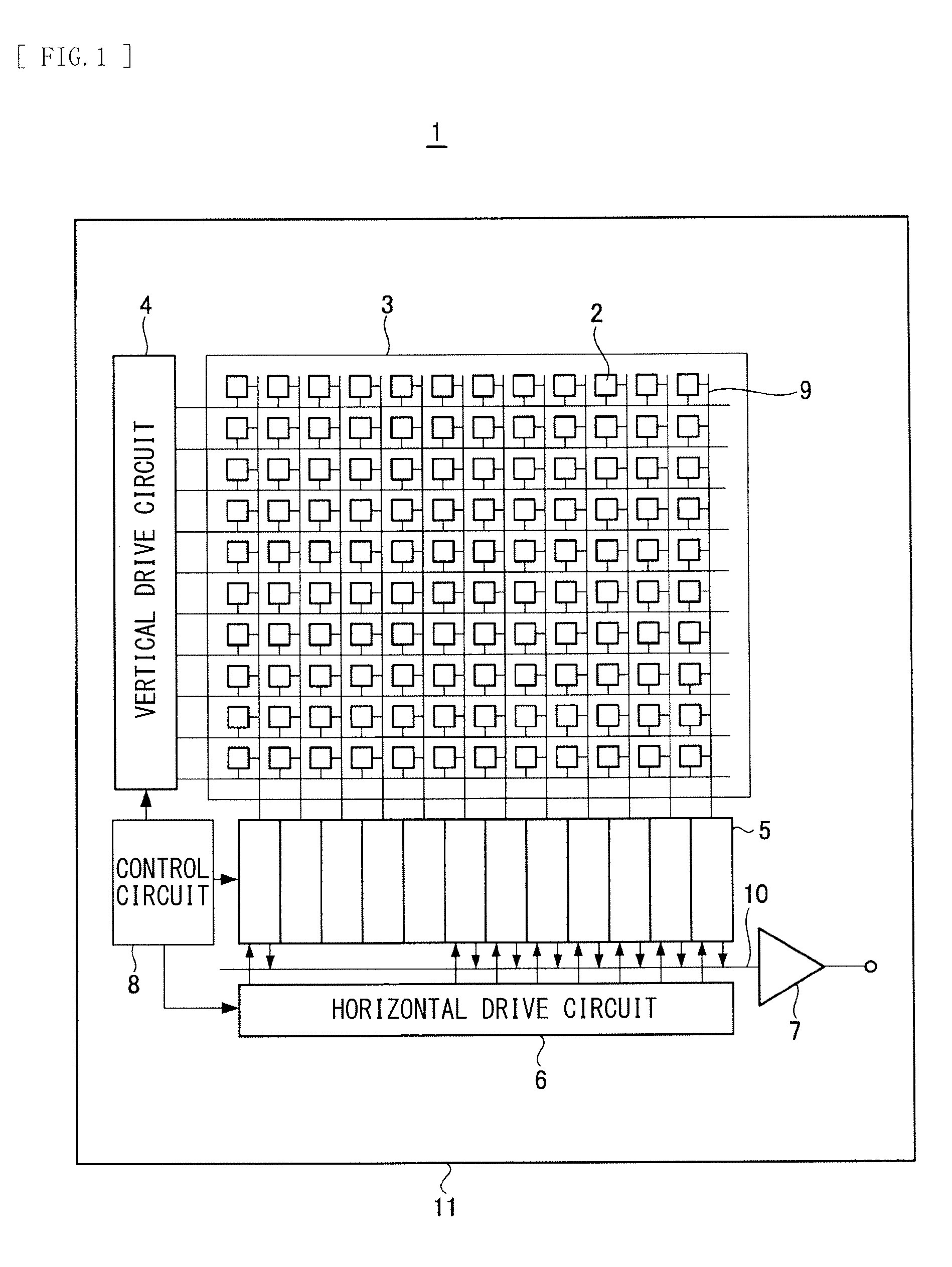
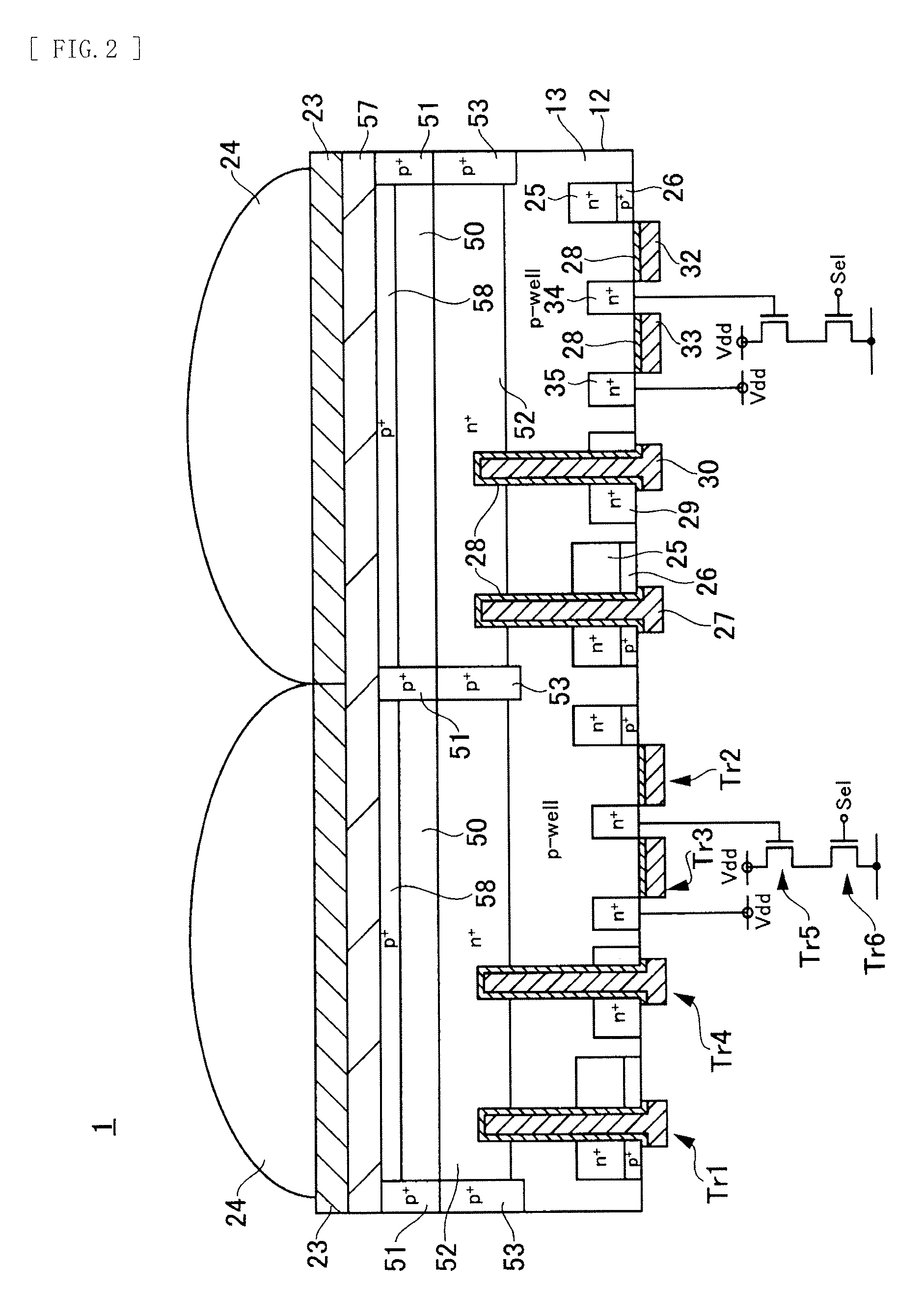
[0079]FIG. 1 illustrates a schematic configuration diagram (a plan view) of a solid-state image pickup unit of a first embodiment.

[0080]In this embodiment, the present technology is applied to a CMOS type image sensor.

[0081]As illustrated in FIG. 1, the solid-state image pickup unit 1 of this embodiment is configured by including a pixel region 3 configured of a plurality of pixels 2 arranged on a substrate 11 made of silicon, a vertical drive circuit 4, a column signal processing circuit 5, a horizontal drive circuit 6, an output circuit 7, and a control circuit 8.

[0082]The pixel 2 is configured of a photoelectric conver...

first modification example

2. First Modification Example of First Embodiment

[0281]In the first embodiment, as illustrated in FIG. 2, the p-type semiconductor layer 58 is formed on the photoelectric conversion section 50.

[0282]On the other hand, the p-type semiconductor layer 58 may be omitted.

[0283]Moreover, the transparent electrode 57 above the photoelectric conversion section 50 may be omitted.

[0284]Further, the photoelectric conversion section-side pixel isolation section 51 that partitions the photoelectric conversion section 50 for each pixel may be omitted.

[0285]Hereinafter, a case where the p-type semiconductor layer, the transparent electrode, and the photoelectric conversion side pixel isolation section are omitted will be described as a first modification example.

[0286]A schematic configuration diagram (a sectional view of a main part) of a solid-state image pickup unit 15 of the first modification example of the first embodiment is illustrated in FIG. 19.

[0287]In FIG. 19, components corresponding ...

second modification example of first embodiment

[0306]In a case where the photoelectric conversion section 50 is formed on the substrate 12 as with the first embodiment, an intermediate layer that reduces a potential barrier may be provided to easily move a signal charge generated by the photoelectric conversion section 50 from the photoelectric conversion section 50 side to the substrate 12 side. Hereinafter, a case where the intermediate layer is provided will be described below as a second modification example.

[0307]A schematic configuration diagram (a sectional view of a main part) of a solid-state image pickup unit 16 of the second modification example of the first embodiment is illustrated in FIG. 22.

[0308]In FIG. 22, components corresponding to those in FIG. 2 are denoted by same numerals, and will not be further described.

[0309]In the solid-state image pickup unit 16 of the second modification example, as illustrated in FIG. 22, an intermediate layer 60 is formed between the substrate 12 and the photoelectric conversion s...


PUM


Abstract

There is configured a solid-state image pickup unit including a photoelectric conversion section formed on a light incident side of a substrate; a first charge accumulation section accumulating a signal charge generated by the photoelectric conversion section; a second charge accumulation section formed in a region other than a light-condensing region where incident light is condensed in the substrate on a side opposite to a light incident side and formed to be laminated together with the first charge accumulation section in a depth direction of the substrate; and a floating diffusion section formed in a region other than the light-condensing region in the substrate on the side opposite to the light incident side and converting the signal charge into a voltage.

Description

TECHNICAL FIELD[0001]The present technology relates to a solid-state image pickup unit. Moreover, the present technology relates to an electronic apparatus including a solid-state image pickup unit.BACKGROUND ART[0002]An example of a solid-state image pickup unit is a CMOS (Complementary Metal Oxide Semicondoctor) type image sensor that reads a photocharge accumulated in a pn junction capacity of a photodiode as a photoelectric conversion device through a MOS transistor.[0003]In this CMOS type image sensor, an operation of reading a photocharge accumulated in the photodiode is executed on each pixel, each row, or the like. Therefore, exposure periods in which the photocharge is accumulated in all pixels are not allowed to coincide with one another, and in a case where a subject is moving, or the like, distortion occurs during image pickup.[0004]Therefore, global exposure in which image pickup is performed on all pixels in a same exposure time is executed.[0005]Then, as one method of...

Claims


Application Information

Patent Timeline
Patent Type & Authority Applications(United States)
IPC IPC(8): H01L27/148
CPCH01L27/14812H01L27/14818H01L27/14612H01L27/1463H01L27/1464H01L27/14689H01L27/14623H01L27/14627H04N25/77
Inventor TODA, ATSUSHI
Owner SONY SEMICON SOLUTIONS CORP
Why Eureka
Try Eureka