Organic Compound, Light-Emitting Element, Display Module, Lighting Module, Light-Emitting Device, Display Device, Electronic Device, and Lighting Device

Inactive Publication Date: 2015-08-27
SEMICON ENERGY LAB CO LTD
View PDF2 Cites 11 Cited by
  • Summary
  • Abstract
  • Description
  • Claims
  • Application Information

AI Technical Summary

Benefits of technology

The present invention provides a novel organic compound that can be used in a light-emitting element. This compound has high triplet excitation level and heat resistance, resulting in high emission efficiency and low power consumption. Additionally, this compound has a small half width of an emission spectrum, high color purity, and a microcavity structure that increases the intensity of light in a blue region. These features make it ideal for use in various electronic devices and lighting modules.

Problems solved by technology

Therefore, in a light-emitting element having a microcavity structure or a color filter, light with relatively high spectral intensity with respect to a non-desired wavelength is mostly diminished or intercepted and thus cannot be extracted.

Method used


Image

  • Organic Compound, Light-Emitting Element, Display Module, Lighting Module, Light-Emitting Device, Display Device, Electronic Device, and Lighting Device
  • Organic Compound, Light-Emitting Element, Display Module, Lighting Module, Light-Emitting Device, Display Device, Electronic Device, and Lighting Device
  • Organic Compound, Light-Emitting Element, Display Module, Lighting Module, Light-Emitting Device, Display Device, Electronic Device, and Lighting Device

Examples


example 1

[0322]In this example, a method of synthesizing N,N′-bis(2,6-dimethylphenyl)-N,N′-bis[3-(9-phenyl-9H-fluoren-9-yl)phenyl]pyrene-1,6-diamine (abbreviation: 1,6oDMemFLPAPrn), which is an organic compound of one embodiment of the present invention, is described. A structural formula of 1,6oDMemFLPAPrn is shown below.

Step 1: Synthesis of N-(2,6-dimethylphenyl)-N-[3-(9-phenyl-9H-fluoren-9-yl)phenyl]amine (abbreviation: oDMemFLPA)

[0323]Into a 200-mL three-neck flask were put 2.7 g (6.9 mol) of 9-(3-bromophenyl)-9-phenyl fluorine and 2.0 g (21.0 mol) of sodium tert-butoxide, and the air in the flask was replaced with nitrogen. Then, 35.0 mL of toluene, 0.9 mL (6.9 mol) of 2,6-dimethylaniline, 0.5 mL of a 10% hexane solution of tri(tert-butyl)phosphine, and 42 mg (0.1 mmol) of bis(dibenzylideneacetone)palladium(0) were added thereto, the temperature of the mixture was set to 90° C. and the mixture was stirred for 13.0 hours. After the stirring, suction filtration through Florisil (produced ...

example 2

[0336]In this example, a light-emitting element of one embodiment of the present invention (Light-emitting element 1) and a Comparative light-emitting element 1 are described. Structure formulae of organic compounds used for Light-emitting element 1 and Comparative light-emitting element 1 are shown below.

(Method of Manufacturing Light-Emitting Element 1)

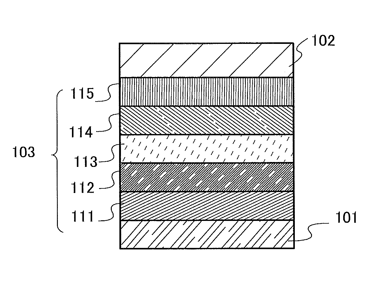
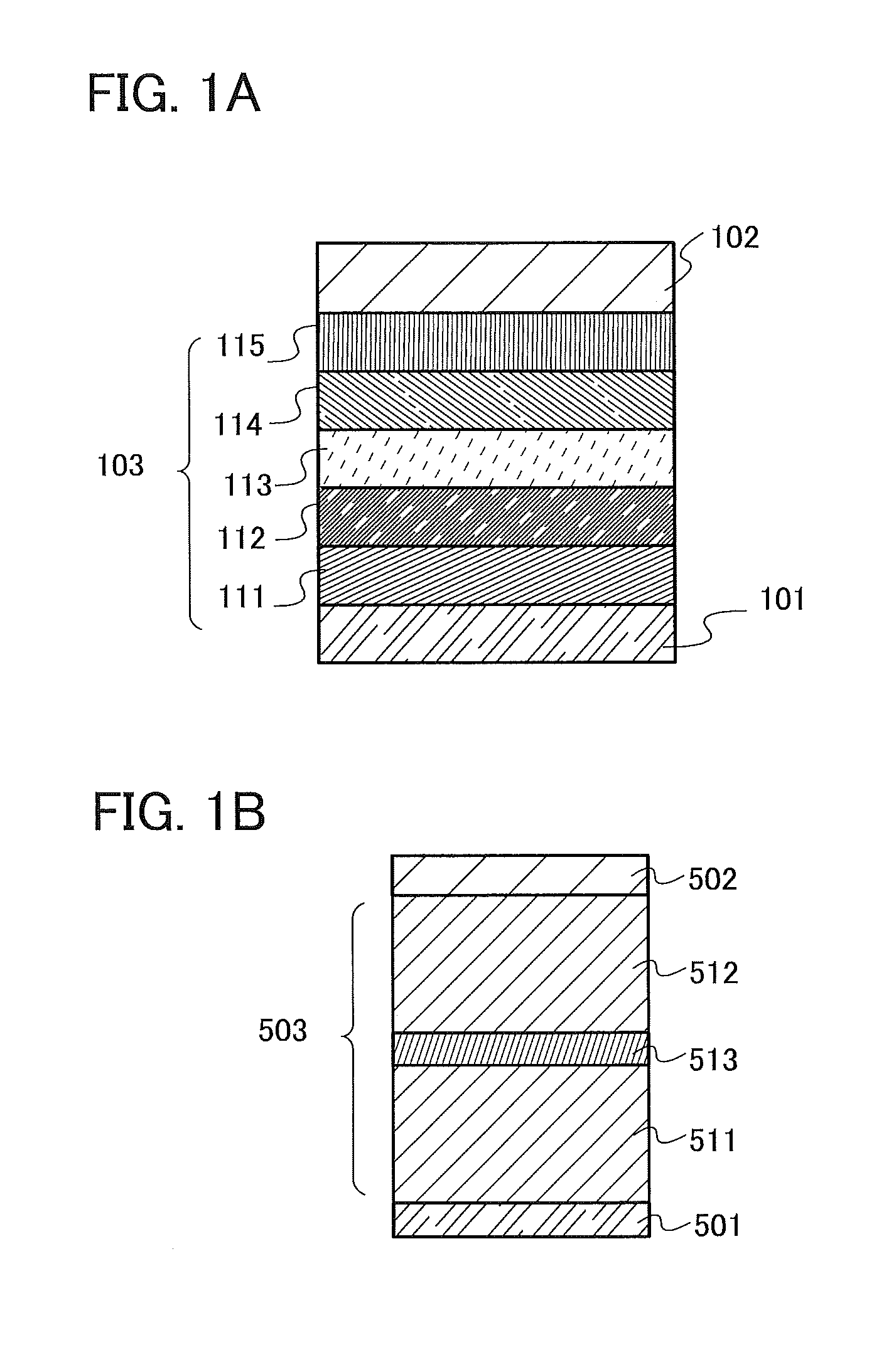
[0337]First, a film of indium tin oxide containing silicon oxide (ITSO) was formed over a glass substrate by a sputtering method, so that the first electrode 101 was formed. The thickness of the first electrode 101 was set to 110 nm and the area of the electrode was set to 2 mm×2 mm. Here, the first electrode 101 is an electrode that functions as an anode of a light-emitting element.

[0338]Next, in pretreatment for forming the light-emitting element over the substrate, a surface of the substrate was washed with water and baked at 200° C. for an hour, and then UV ozone treatment was performed for 370 seconds.

[0339]Then, the substrate ...

example 3

[0354]In this example, a method of synthesizing N,N′-bis[3-(dibenzofuran-4-yl)-2,6-dimethylphenyl]-N,N′-diphenylpyrene-1,6-diamine (abbreviation: 1,6mFrBAPrn-04), which is an organic compound of one embodiment of the present invention, is described. A structural formula of 1,6mFrBAPrn-04 is shown below.

Step 1: Synthesis of N-[3-(dibenzofuran-4-yl)-2,6-dimethylphenyl]-N-phenylamine (abbreviation: mFrBA-04)

[0355]Into a 200-mL three-neck flask was put 5.2 g (26.1 mmol) of 3-bromo-2,6-dimethylaniline, and the air in the flask was replaced with nitrogen. To this flask were added 98.0 mL of toluene, 32.0 mL of ethanol, 6.6 g (31.3 mmol) of 4-dibenzofuran boronic acid, 0.4 g (1.3 mmol) of tris(2-methylphenyl)phosphine, and 25.8 mL of a potassium carbonate solution (2 mol / L). The mixture was degassed, and 0.09 g (0.4 mmol) of palladium(II) acetate was added thereto. The mixture was stirred at 90° C. for 15.5 hours. After the stirring, toluene and water were added to the mixture, an organic ...


PUM

PropertyMeasurementUnit
Widthaaaaaaaaaa
Wavelengthaaaaaaaaaa
Energyaaaaaaaaaa

Abstract

A light-emitting element with high emission efficiency. The light-emitting element includes a pair of electrodes and an EL layer between the pair of electrodes. In the light-emitting element, the EL layer contains at least a light-emitting material, the light-emitting material is a 1,6-bis(diphenylamino)pyrene derivative, and a structural change between an excited state and a ground state in the 1,6-bis(diphenylamino)pyrene derivative is smaller than that in a 1,6-bis(diphenylamino)pyrene derivative in which hydrogen is bonded to ortho positions of two phenyl groups of each of two diphenylamino groups.

Description

BACKGROUND OF THE INVENTION[0001]1. Field of the Invention[0002]One embodiment of the present invention relates to an organic compound, and a light-emitting element, a display module, a lighting module, a display device, a light-emitting device, an electronic device, and a lighting device each including the organic compound. Note that one embodiment of the present invention is not limited to the above technical field. The technical field of one embodiment of the invention disclosed in this specification and the like relates to an object, a method, or a manufacturing method. In addition, one embodiment of the present invention relates to a process, a machine, manufacture, or a composition of matter. Specifically, examples of the technical field of one embodiment of the present invention disclosed in this specification include a semiconductor device, a display device, a liquid crystal display device, a light-emitting device, a lighting device, a power storage device, a storage device,...

Claims


Application Information

Patent Timeline
IPC IPC(8): H01L51/00C07D307/91C07C211/61
CPCH01L51/006C07C211/61H01L51/0058C07D307/91H01L51/0061H01L51/5092H01L51/5012H01L51/5024C07C2103/50H01L51/5072H01L51/0073C07C2603/18C07C2603/50H10K85/636H10K85/633H10K85/6574H10K50/11H10K2101/20C07C211/54C07C211/57C09K11/06H10K85/622
Inventor OGITA, KAORISUZUKI, TSUNENORIHASHIMOTO, NAOAKIHAMADA, TOSHIKISUZUKI, KUNIHIKOHOSOUMI, SHUNSUKESEO, SATOSHI
Owner SEMICON ENERGY LAB CO LTD
Why Eureka
Try Eureka