Method for forming pn junction in graphene with application of DNA and pn junction structure formed using the same

Active Publication Date: 2015-08-27
KOREA INST OF SCI & TECH
View PDF2 Cites 9 Cited by
  • Summary
  • Abstract
  • Description
  • Claims
  • Application Information

AI Technical Summary

Benefits of technology

[0009]Graphene is gaining much attention because of its excellent electrical and mechanical properties, but has unreliable semiconductor properties due to its lack of an energy band gap. According to an aspect, the present disclosure is direct

Problems solved by technology

However, contrary to silicon which is a semiconductor, graphene has no gap between a valence band and a conduction band.
However, graphene doping by a diffusion process precludes localized doping in only a desired region, and thus, becomes an obstacle to integration of devices.
Also, a graphene surface doping process by an ion implantation technique generates a lattice defect in graphene by ion collision, which reduces electron mobility of graphene.
Further, these processes have disadvantages in that they require a high temp

Method used


Image

  • Method for forming pn junction in graphene with application of DNA and pn junction structure formed using the same
  • Method for forming pn junction in graphene with application of DNA and pn junction structure formed using the same
  • Method for forming pn junction in graphene with application of DNA and pn junction structure formed using the same

Examples


Embodiment Construction

[0018]Hereinafter, embodiments of the present disclosure will be described in detail with reference to the accompanying drawings. Prior to the description, it should be understood that the terms or words used in the specification and the appended claims should not be construed as limited to general and dictionary meanings, but interpreted based on the meanings and concepts corresponding to technical aspects of the present disclosure on the basis of the principle that the inventor is allowed to define terms appropriately for the best explanation.

[0019]Therefore, embodiments described in the specification and illustrations shown in the drawings are just examples of the present disclosure, and do not fully represent the technical aspects of the disclosure, so it should be understood that other equivalents and modifications could be made thereto.

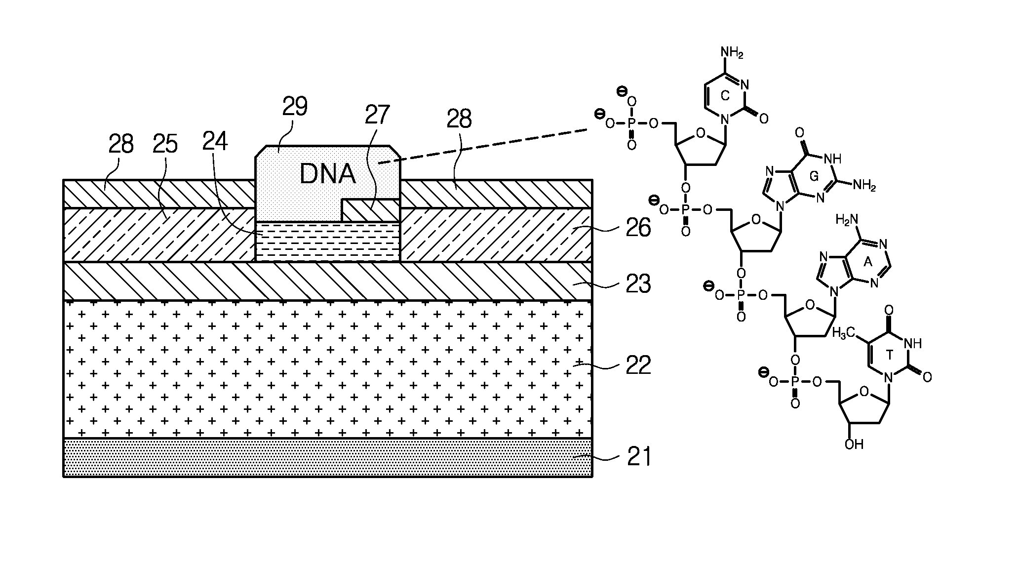
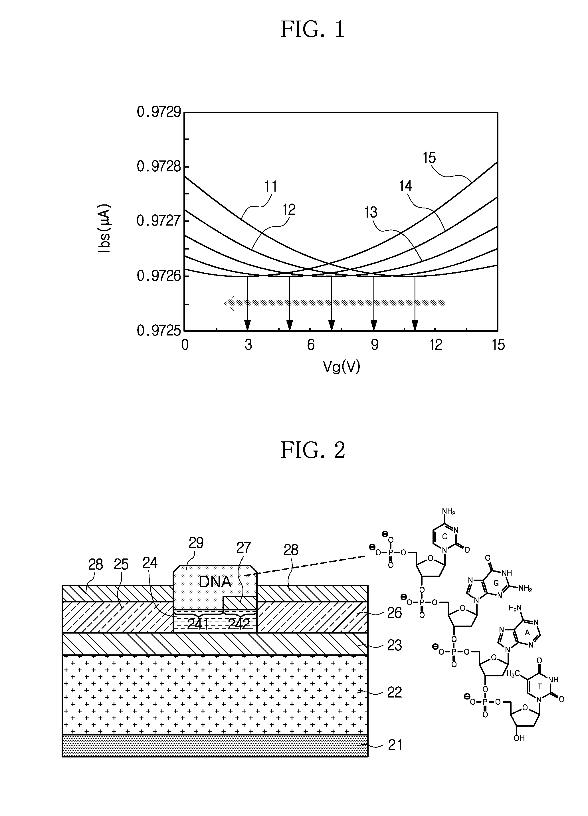
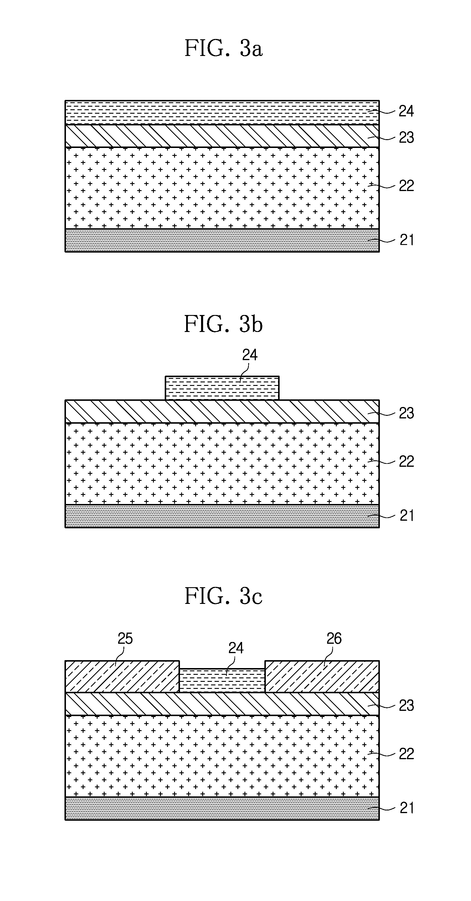
[0020]The embodiments of the present disclosure are configured to provide a chemical doping effect to a surface of graphene using electrical pr...


PUM


Abstract

A method for forming a PN junction in graphene includes: forming a graphene layer, and forming a DNA molecule layer on a partial region of the graphene layer, the DNA molecule layer having a nucleotide sequence structure designed to provide the graphene layer with a predetermined doping property upon adsorption on the graphene layer. The DNA molecule has a nucleotide sequence structure designed for doping of graphene so that doped graphene has a specific semiconductor property. The DNA molecule is coated on the surface of the graphene layer of which the partial region is exposed by micro patterning, and thereby, PN junctions of various structures may be formed by a region coated with the DNA molecule and a non-coated region in the graphene layer.

Description

CROSS-REFERENCE TO RELATED APPLICATION[0001]This application claims priority to Korean Patent Application No. 10-2014-0021412, filed on Feb. 24, 2014, and all the benefits accruing therefrom under 35 U.S.C. §119, the contents of which in its entirety are herein incorporated by reference.BACKGROUND[0002]1. Field[0003]Embodiments relate to a method for forming a PN junction in graphene through the application of DNA and a PN junction structure formed thereby. More particularly, embodiments relate to formation of an organic material-based semiconductor junction structure by coating a nucleotide sequence-controllable DNA molecule on a graphene surface.[0004]2. Description of the Related Art[0005]A PN junction refers to a boundary or an interface between two regions exhibiting a p-type property and an n-type property inside a semiconductor. The PN junction is a key structure of many semiconductor devices because it can perform lots of important functions. In case an electric current flow...

Claims


Application Information

Patent Timeline
IPC IPC(8): H01L51/05H01L51/10H01L51/00
CPCH01L51/0558H01L51/0012H01L51/0093H01L51/107H01L51/002C01B32/194H10K85/20H10K85/761H10K10/486H10K10/26H10K10/484H10K10/88H10K71/30H10K71/191
Inventor KIM, CHULKIKIM, YEONG JUNJUNG, YOUNG MOJUN, SEONG CHANLEE, TAIKJINLEE, SEOKBYUN, YOUNG TAEWOO, DEOK HAKIM, SUN HOSEO, MIN AHKIM, JAE HUNYI, JONG CHANG
Owner KOREA INST OF SCI & TECH
Why Eureka
Try Eureka