

Light emitting element, light emitting device, authentication device, and electronic device
a technology of light emitting devices and light emitting elements, which is applied in the direction of thermoelectric device junction materials, semiconductor devices, electrical devices, etc., can solve the problems of not having a high efficiency and long life element that emits light in the near-infrared region before, and achieves superior reliability, long life, and high efficiency
- Summary
- Abstract
- Description
- Claims
- Application Information
AI Technical Summary
Benefits of technology
Problems solved by technology
Method used
Image

Examples
working examples
[0217]Next, specific working examples according to aspects of the invention will be described.
[0218]1. Production of Light Emitting Material
[0219]A pyrromethene-based boron complex represented by the formula IRD-1 was synthesized through the following steps 1 to 6.
[0220]Step 1: Synthesis of ethyl ester (5-methyl-thiophene-2-carboxylic acid ethyl ester)
[0221]2-Methyl thiophene (1.7 g, 0.175 mol) was added to dehydrated THF (150 ml) in a 1-liter three-neck flask under an Ar gas flow, and the mixture was cooled to −65° C. Then, a 1.6 M hexane solution of n-BuLi (120 ml, 0.19 mol) was dripped therein at a temperature of −60° C. or lower, and the mixture was stirred for 1 hour as is.
[0222]Then, 2-ethyl chloroformate (C2H5OCOCl: 2.1 g, 0.19 mol) was added to dehydrated THF (10 ml), and the mixture was cooled to −55° C. or lower. This solution was dripped into the former solution at a temperature of −50° C. or lower. After the end of the dripping, cooling of the reaction solution was stopp...
working example 1
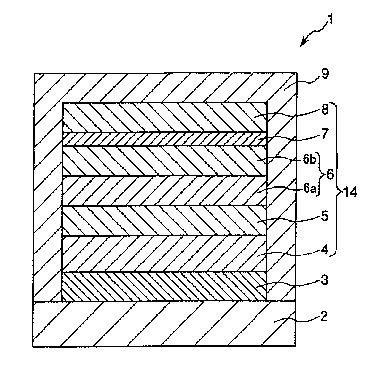
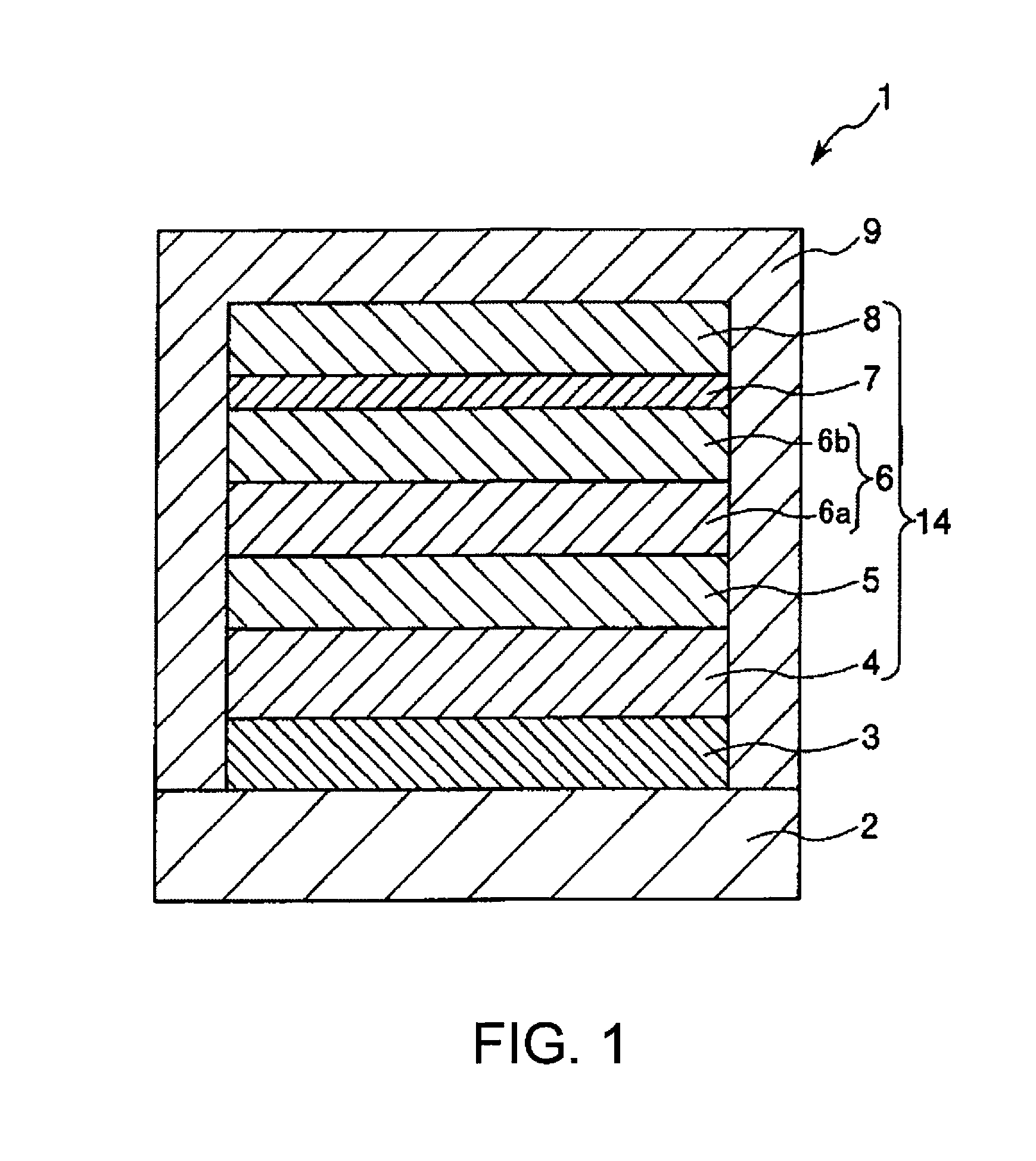
[0241] First, a transparent glass substrate having an average thickness of 0.5 mm was prepared. Next, an ITO electrode (anode) having an average thickness of 100 nm was formed on this substrate by a sputtering method.
[0242]The substrate was subjected to ultrasonic cleaning while being immersed in acetone and 2-propanol in this order, and then oxygen plasma treatment and argon plasma treatment were performed thereon. These plasma treatments were performed under conditions in which the plasma power was 100 W, the flow rate of the gas was 20 sccm, and the treatment time was 5 seconds in a state in which the substrate was heated to 70 to 90° C.
[0243] The compound represented by the formula HTL-1 was deposited on the ITO electrode by a vacuum deposition method to form a positive hole injecting layer having an average thickness of 50 nm.
[0244] The component material of the light emitting layer was deposited on the positive hole injecting layer by a vacuum deposition method to form a light...
working example 2
[0250]A light emitting element was produced in the same manner as in Working Example 1, except that the content (doping concentration) of the light emitting material (dopant) in the light emitting layer was set to 0.5 wt %.
PUM
 Abstract
Description
Claims
Application Information