Silicon Photomultiplier Based TOF-PET Detector

a photomultiplier and detector technology, applied in the field of nuclear medical imaging, can solve the problems of inability to accurately detect the total pet system performance, the timing resolution loss of these events is inevitable, and the complexity and high electronic density and power add to the complexity. , to achieve the effect of reducing the complexity and power requirements of the electronic circuit, easing the necessary fabrication methods, and recovering detection efficiency

Active Publication Date: 2015-10-08
SIEMENS MEDICAL SOLUTIONS USA INC
View PDF6 Cites 53 Cited by
  • Summary
  • Abstract
  • Description
  • Claims
  • Application Information

AI Technical Summary

Benefits of technology

[0018]Various embodiments relate to a scintillation block detector that employs an array of optically air-coupled scintillation pixels, the array being wrapped in reflector material and optically coupled to an array of silicon photomultiplier (SiPM) light sensors with common-cathode signal timing pickoff and individual anode signal position and energy determination. The design features afford an optimized combination of photopeak energy event sensitivity and timing, while reducing electronic circuit complexity and power requirements, and easing necessary fabrication methods. Four of these small blocks, or “miniblocks,” can be combined as optically and electrically separated quadrants of a la...

Problems solved by technology

However, a number of practical and technical issues make this both difficult and sub-optimal for total PET system performance.
Scatter of 511 keV gammas between scintillator pixels is frequent, and although a system design might recover adjacent coincident events adding to the total energy, this would add to complexity and high electronic density and power,...

Method used


Image

  • Silicon Photomultiplier Based TOF-PET Detector
  • Silicon Photomultiplier Based TOF-PET Detector
  • Silicon Photomultiplier Based TOF-PET Detector

Examples


Embodiment Construction

[0052]The present invention may be understood more readily by reference to the following detailed description of preferred embodiments of the invention as well as to the examples included therein. All numeric values are herein assumed to be modified by the term “about,” whether or not explicitly indicated. The term “about” generally refers to a range of numbers that one of skill in the art would consider equivalent to the recited value (i.e., having the same function or result). In many instances, the term “about” may include numbers that are rounded to the nearest significant figure.

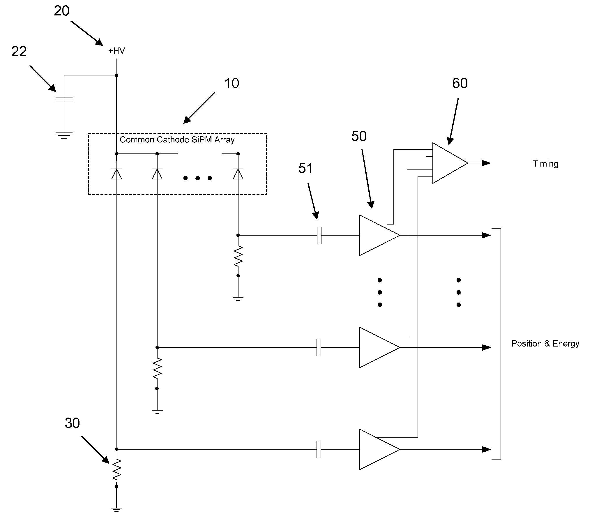
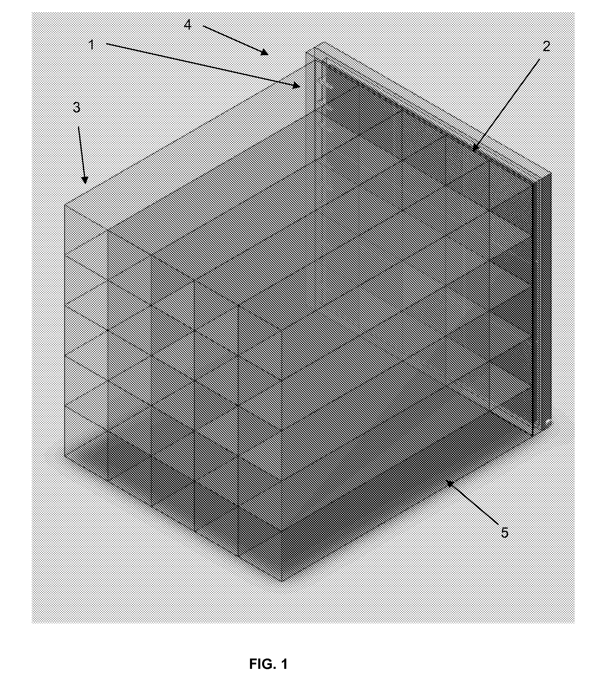
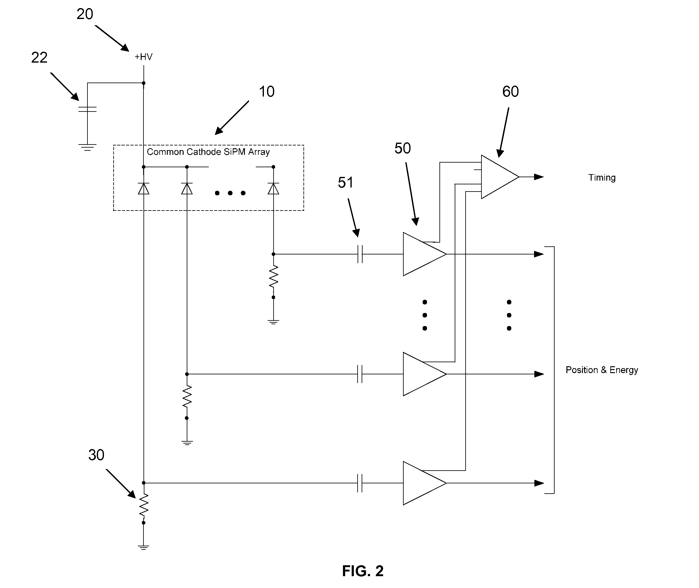
[0053]The miniblock detector described here comprises an array of silicon photomultipliers (SiPMs), which may be monolithic, discrete or multiple monolithic devices in a package, optically coupled to a block of scintillator pixels without inter-pixel reflectors (“air coupled”), or with few inter-pixel reflectors, and surrounded by a thin efficient optical reflector. Air coupling between scintillator pix...


PUM


Abstract

A scintillation block detector employs an array of optically air coupled scintillation pixels, the array being wrapped in reflector material and optically coupled to an array of silicon photomultiplier light sensors with common-cathode signal timing pickoff and individual anode signal position and energy determination. The design features afford an optimized combination of photopeak energy event sensitivity and timing, while reducing electronic circuit complexity and power requirements, and easing necessary fabrication methods. Four of these small blocks, or “miniblocks,” can be combined as optically and electrically separated quadrants of a larger single detector in order to recover detection efficiency that would otherwise be lost due to scattering between them. Events are validated for total energy by summing the contributions from the four quadrants, while the trigger is generated from either the timing signal of the quadrant with the highest energy deposition, the first timing signal derived from the four quadrant time-pickoff signals, or a statistically optimum combination of the individual quadrant event times, so as to maintain good timing for scatter events. This further reduces the number of electronic channels required per unit detector area while avoiding the timing degradation characteristic of excessively large SiPM arrays.

Description

BACKGROUND OF THE INVENTION[0001]1. Field of the Invention[0002]The present invention relates generally to nuclear medical imaging, and in particular relates to scintillation detectors used in Positron Emission Tomography (PET).[0003]2. Description of the Related Art[0004]Silicon photomultipliers (SiPMs) can be used to improve the timing performance of positron emission tomography (PET) detectors over that achievable with conventional vacuum tube photomultipliers (PMTs). Some of the properties of these devices contributing to this are the high photon detection efficiency (PDE), a combination of high microcell fill factor and very high quantum efficiency (QE), high uniformity of microcell gain and good single photon time response. The small size of SiPMs allows finer sampling of pixelated or monolithic scintillator blocks, even down to one-to-one coupling of light sensor and scintillator pixel. This can reduce the light spread to the sensors required for event positioning which can r...

Claims


Application Information

Patent Timeline
IPC IPC(8): G01T1/208G01T1/29A61B6/00G01R33/48A61B6/03G01T1/161G01T1/16
CPCG01T1/208G01T1/161G01T1/2985A61B6/4417G01R33/481A61B6/037A61B6/032G01T1/1606A61B6/4233A61B6/4241A61B6/4258G01T1/1647G01T1/20183G01T1/20185G01T1/20184
Inventor MINTZER, ROBERT A.ARNOTT, JAMES CHRISTOPHERAYKAC, MEHMETBREUER, JOHANNESCHO, SANGHEEHANSEN, PETERKAPUSTA, MACIEJ P.CORBEIL, JAMES L.ZHANG, NAN
Owner SIEMENS MEDICAL SOLUTIONS USA INC
Why Eureka
Try Eureka