
Directed self-assembly pattern formation methods and compositions

a technology of composition and self-assembly, applied in the field of electronic device manufacturing, can solve the problems of inconvenient use of tools, difficulty in directly creating patterns beyond about 36 nm half-pitch line and space patterns, and inability to meet the requirements of the application of the technology,

Active Publication Date: 2015-10-08
ROHM & HAAS ELECTRONICS MATERIALS LLC +1
View PDF13 Cites 24 Cited by
  • Summary
  • Abstract
  • Description
  • Claims
  • Application Information

AI Technical Summary

Benefits of technology

This patent describes methods for making patterns on semiconductor devices using a process called directed self-assembly. The methods involve applying a special layer of material called a crosslinkable underlayer, which is then heated to form a crosslinked underlayer. A layer of a special polymer called a block copolymer is then placed on top of this crosslinked underlayer and annealed to create the pattern. These methods can make very precise patterns, which are useful in the manufacture of semiconductor devices.

Problems solved by technology

The physical resolution limit of this process, however, makes it difficult to directly create patterns beyond about 36 nm half-pitch line and space patterns.
While EUV optical exposure tools are being developed for creating higher resolution patterns, the cost of such tools is prohibitive and adoption of the technology remains uncertain.
Widespread use in DSA underlayers of polymers containing vinyl BCB, however, is limited by the requirement of a relatively high annealing temperature (e.g., about 250° C.) and / or long annealing time to induce crosslinking by isomerization of the cyclobutene ring to the reactive o-quinodimethane intermediate.
The use of high crosslinking temperatures can adversely impact underlying layers including, for example, antireflective coating and hardmask layers by causing thermal degradation and / or oxidation of those layers.
The high crosslinking temperatures can further give rise to dewetting, resulting in poor pattern formation, and to oxidation-induced surface energy changes.
In addition, a higher crosslinking temperature would limit the types of functional monomers that could otherwise be used in a DSA underlayer layer composition.
High crosslinking temperatures are also disadvantageous in that a more complicated heating tool may be required to process the substrates to provide an inert gas environment to prevent unwanted oxidation that could results in an increase in surface energy of the underlayer.

Method used

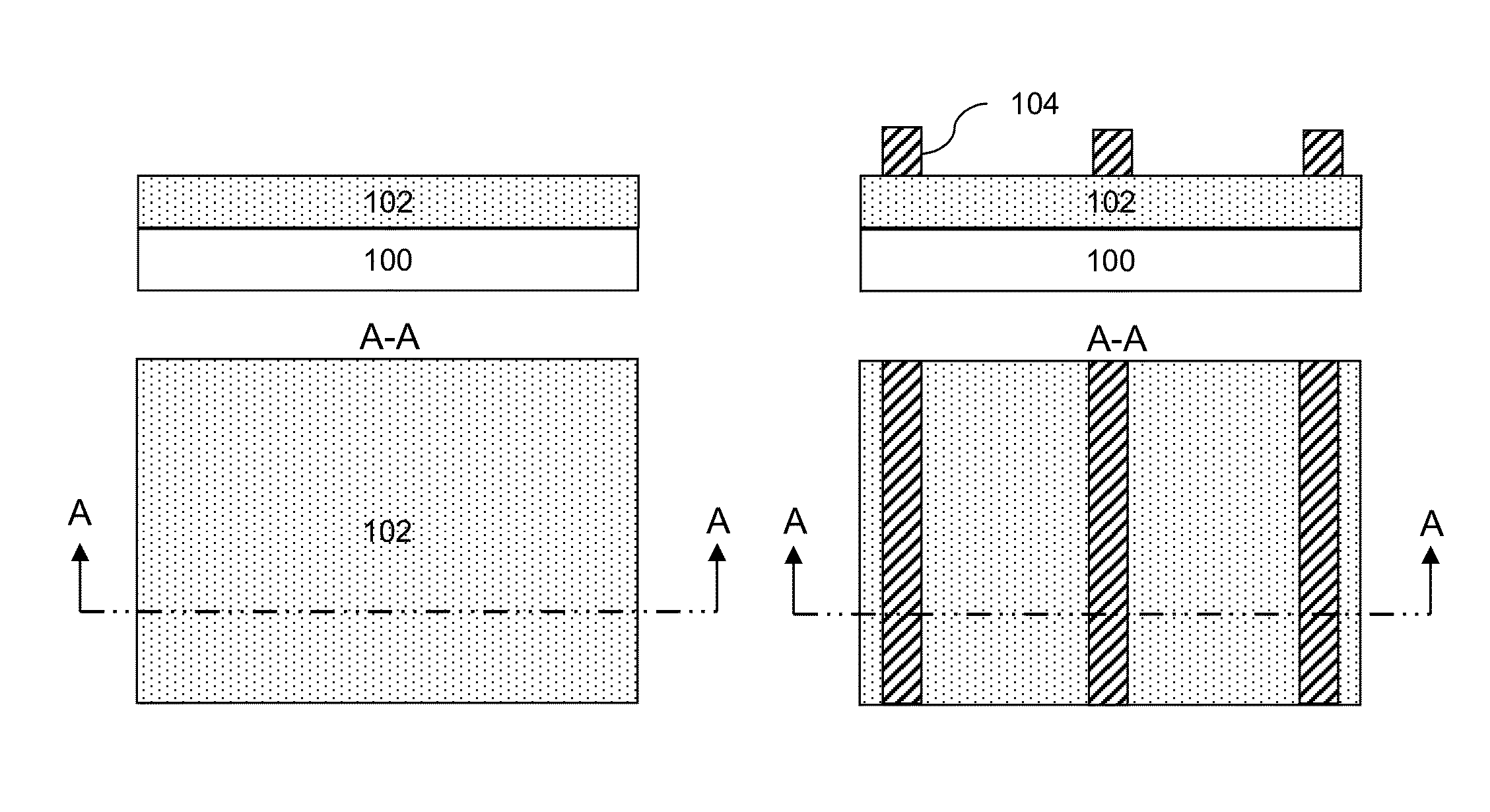
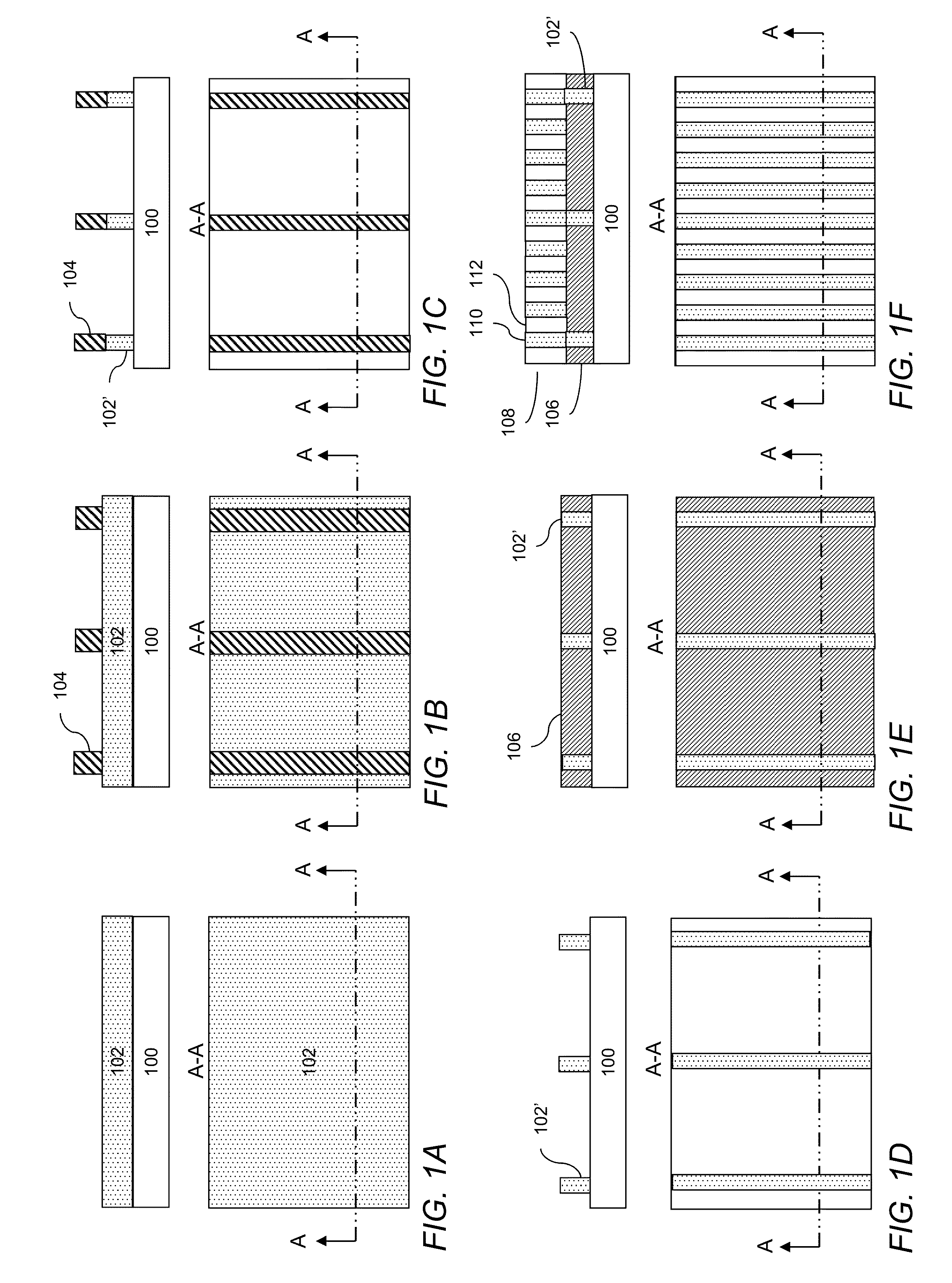

Image

  • Directed self-assembly pattern formation methods and compositions
  • Directed self-assembly pattern formation methods and compositions
  • Directed self-assembly pattern formation methods and compositions

Examples


example 1

Crosslinkable Polymer 1 (CP1) (Comparative)

[0056]Styrene and 4-vinylbenzocyclobutene (VBCB) monomers were passed through an alumina column to remove all the inhibitors. 28.883 g of styrene, 1.116 g of VBCB, 0.225 g of N-tert-butyl-N-(2-methyl-1-phenylpropyl)-O-(1-phenylethyl)hydroxylamine, and 0.011 g of 2,2,5-Trimethyl-4-phenyl-3-azahexane-3-nitroxide were charged into a 100 mL Schlenk flask. The reaction mixture was degassed by three freeze-pump-thaw cycles and then the flask was charged with nitrogen and sealed. Subsequently, the reaction flask was heated at 120° C. for 19 hours. Precipitation was carried out in methanol / water (80 / 20). Precipitated polymers were collected by filtration, air-dried overnight, re-dissolved in THF, and re-precipitated into methanol / water (80 / 20). The final polymer was filtered, air-dried overnight and further dried under vacuum at 25° C. for 48 hours to give Crosslinkable Polymer 1 (CP1).

example 2

Crosslinkable Polymer 2 (CP2) (Comparative)

[0057]Styrene and 4-vinylbenzocyclobutene (VBCB) monomers were passed through an alumina column to remove all the inhibitors. 26.341 g of styrene, 3.658 g of VBCB, 0.229 g of N-tert-butyl-N-(2-methyl-1-phenylpropyl)-O-(1-phenylethyl)hydroxylamine, and 0.011 g of 2,2,5-Trimethyl-4-phenyl-3-azahexane-3-nitroxide were charged into a 100 mL Schlenk flask. The reaction mixture was degassed by three freeze-pump-thaw cycles and then the flask was charged with nitrogen and sealed. Subsequently, the reaction flask was heated at 120° C. for 19 hours. Precipitation was carried out in methanol / water (80 / 20). Precipitated polymers were collected by filtration, air-dried overnight, re-dissolved in THF, and re-precipitated into methanol / water (80 / 20). The final polymer was filtered, air-dried overnight and further dried under vacuum at 25° C. for 48 hours to give Crosslinkable Polymer 2 (CP2).

example 3

Crosslinkable Polymer 3 (CP3)

[0058]17.899 g of styrene and 2.101 g of 2-(1,2-dihydrocyclobutabenzen-1-yloxy)ethyl methacrylate (BCBMA) were dissolved in 30.000 g of propylene glycol methyl ether acetate (PGMEA). The monomer solution was degassed by bubbling with nitrogen for 20 min. PGMEA (15.097 g) was charged into a 250 mL three-neck flask equipped with a condenser and a mechanical stirrer and was degassed by bubbling with nitrogen for 20 min. Subsequently, the solvent in the reaction flask was brought to a temperature of 80° C. V601 (dimethyl-2,2-azodiisobutyrate) (1.041 g) was dissolved in 4.000 g of PGMEA and the initiator solution was also degassed by bubbling with nitrogen for 20 min. The initiator solution was added into the reaction flask and then the monomer solution was fed into the reactor drop-wise over a 3 hour period under rigorous stirring and nitrogen environment. After monomer feeding was complete, the polymerization mixture was left standing for an additional hour...


PUM


Abstract

A method of forming a pattern by directed self-assembly, comprising: (a) providing a semiconductor substrate comprising one or more layers to be patterned; (b) applying a crosslinkable underlayer composition over the one or more layers to be patterned to form a crosslinkable underlayer, wherein the crosslinkable underlayer composition comprises a crosslinkable polymer comprising a first unit of the following general formula (I-A) or (I-B):wherein: P is a polymerizable functional group; L is a single bond or an m+1-valent linking group; X1 is a monovalent electron donating group; X2 is a divalent electron donating group; Ar1 and Ar2 are trivalent and divalent aryl groups, respectively, and carbon atoms of the cyclobutene ring are bonded to adjacent carbon atoms on the same aromatic ring of Ar1 or Ar2; m and n are each an integer of 1 or more; and each R1 is independently a monovalent group; (c) heating the crosslinkable underlayer to form a crosslinked underlayer; (d) forming a self-assembling layer comprising a block copolymer over the crosslinked underlayer; and (e) annealing the self-assembling layer. The methods and compositions find particular applicability in the manufacture of semiconductor devices or data storage devices for the formation of high resolution patterns.

Description

[0001]This application claims the benefit of priority under 35 U.S.C. §119(e) to U.S. Provisional Application No. 61 / 922,767, filed Dec. 31, 2013, the entire contents of which are incorporated herein by reference.FIELD[0002]The invention relates generally to the manufacture of electronic devices. More specifically, this invention relates to methods of forming patterns by directed self-assembly and to underlayer compositions for use in such methods. The methods and compositions have applicability, for example, to semiconductor device manufacturing for the formation of fine patterns, or for data storage such as hard drive manufacture.INTRODUCTION[0003]In the semiconductor manufacturing industry, optical lithography with photoresist materials has been the standard for transferring an image to one or more underlying layers, such as metal, semiconductor and dielectric layers, disposed on a semiconductor substrate, and to the substrate itself. To increase the integration density of semico...

Claims


Application Information

Patent Timeline
IPC IPC(8): H01L21/02H01L21/311
CPCH01L21/02255H01L21/311H01L21/02118C08F212/12C09D125/08C09D125/16G03F7/00H01L21/02282G03F7/0002C08F12/32C08F212/08C08F220/1803C08F220/1807C08F220/1806C08F220/301G03F7/40H01L21/0274G03F7/004G03F7/20G03F7/38C08F212/32C08F220/302
Inventor PARK, JONG KEUNSUN, JIBINGILMORE, CHRISTOPHER D.ZHANG, JIEQIANHUSTAD, PHILLIP D.TREFONAS, III, PETERO'CONNELL, KATHLEEN M.
Owner ROHM & HAAS ELECTRONICS MATERIALS LLC
Learn More