Piezoelectric device, piezoelectric actuator, piezoelectric sensor, hard disk drive, and inkjet printer apparatus
a piezoelectric actuator and actuator technology, applied in the direction of piezoelectric/electrostrictive devices, piezoelectric/electrostrictive/magnetostrictive devices, device material selection, etc., can solve the problems of reducing the reliability and the reliability of the piezoelectric actuator and the piezoelectric sensor according to the present invention, affecting the reliability of the piezoelectric actuator and the piezoelectric sensor, and affecting the production efficiency of the devi
- Summary
- Abstract
- Description
- Claims
- Application Information
AI Technical Summary
Benefits of technology
Problems solved by technology
Method used
Image
Examples
example 1
[0099]In the present example, a term “base member” refers to a member to be provided with a film in each step.
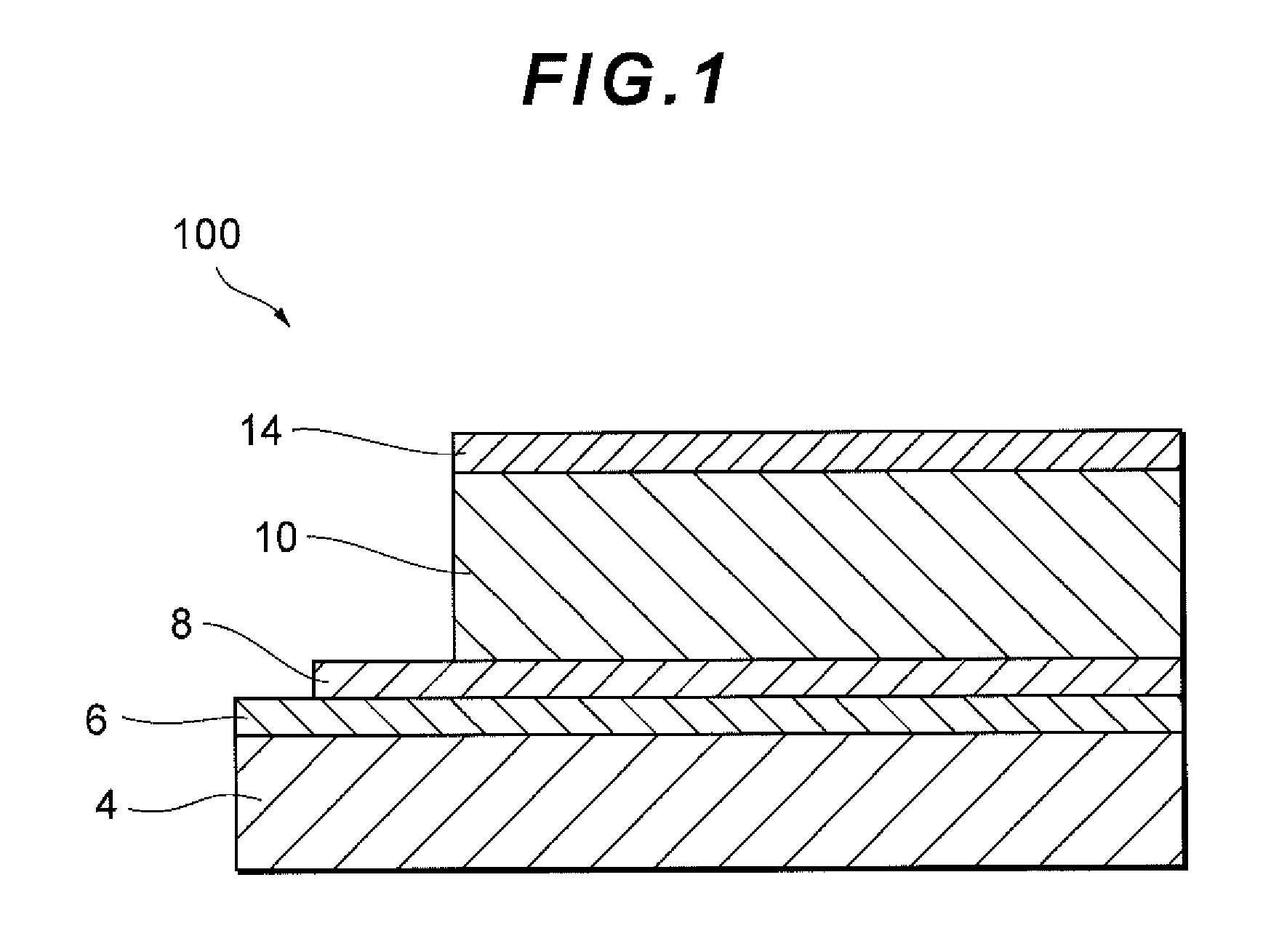
[0100]A silicon wafer (substrate 4) which exhibited (100) face orientation and which had a diameter of 3 inches was placed in a vacuum chamber of a vacuum evaporation apparatus, and evacuation was performed. Thereafter, a film of YSZ (7 percent by mole Y2O3—ZrO2) was formed as an oxide layer 6 and a film of Pt was formed as a lower electrode 8. The base member temperature in film formation was specified to be 900° C. as for YSZ and 700° C. as for Pt. The thickness of the oxide layer 6 was specified to be 10 nm and the thickness of the lower electrode 8 was specified to be 200 nm.
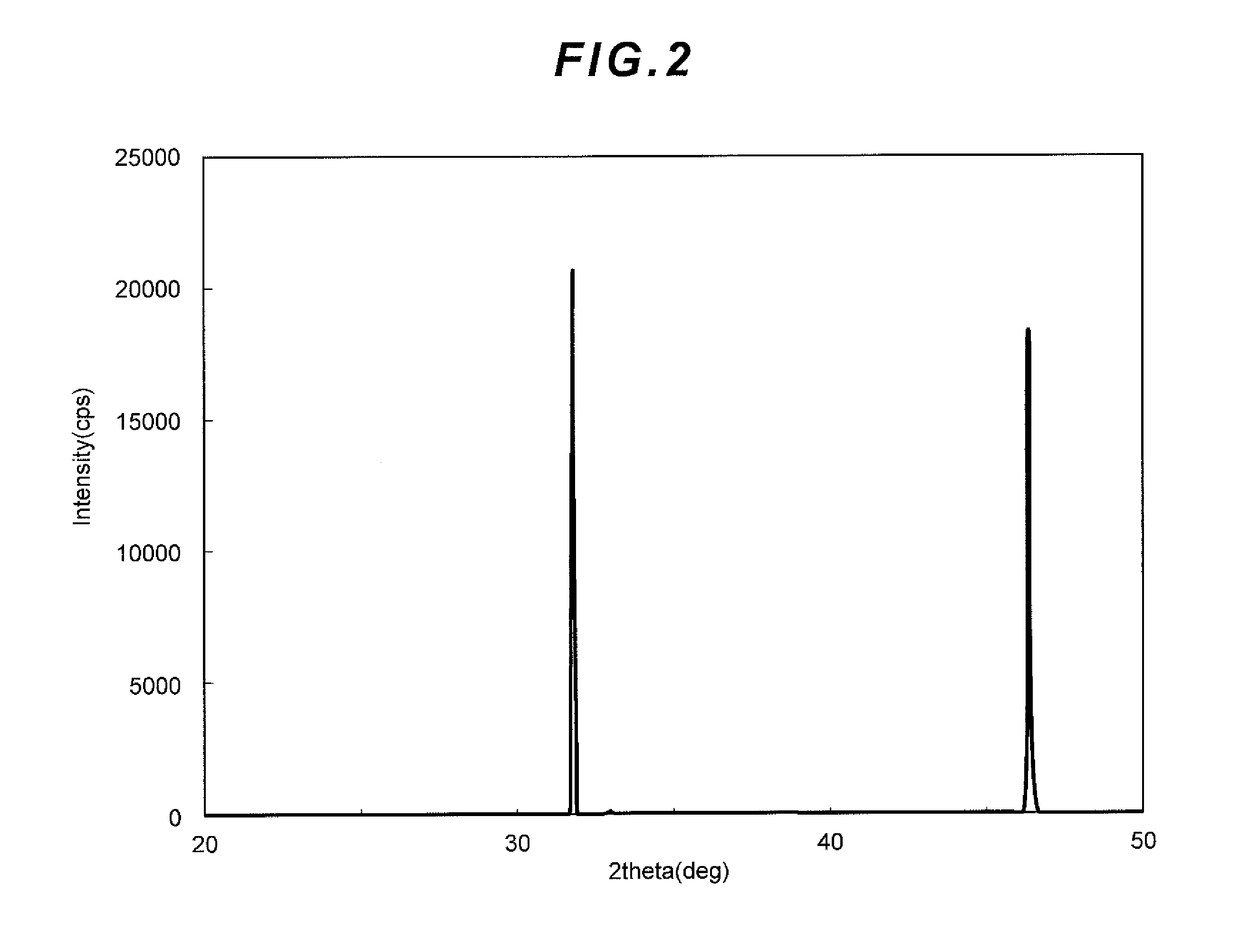
[0101]After the film of the lower electrode 8 was formed, an out-of-plane XRD (X-ray diffraction) measurement was performed to examine the orientation property of the lower electrode 8 in a direction perpendicular to the plane. The out-of-plane XRD measurement is divided into a symmetric reflection m...
example 2
[0107]In Example 1, after the film of the lower electrode was formed, the base material was transferred to another chamber of the RF sputtering apparatus without applying ashing and etching, and evacuation was performed. Then, a potassium-sodium niobate thin film was formed as a piezoelectric layer. As for the sputtering target, a potassium-sodium niobate sintered material containing 0.8 percent by mole of Mn was used. The base member temperature in film formation was specified to be 950° C. and the thickness of the piezoelectric layer was specified to be 3,200 nm. Examination of the orientation property of the piezoelectric layer and production of the piezoelectric element were performed in the same manner as that in Example 1.
example 3
[0108]A MgO substrate (substrate 4) which exhibited (100) face orientation and which had a size of 15 mm×15 mm×0.5 mm was placed in a vacuum chamber of a RF sputtering apparatus, and a film of Pt was formed as a lower electrode 8. The base member temperature in film formation was specified to be 700° C. The thickness of the lower electrode 8 was specified to be 200 nm.
[0109]After the film of the lower electrode 8 was formed, the out-of-plane XRD measurement was performed to examine the orientation property of the lower electrode 8 in a direction perpendicular to the plane. The out-of-plane XRD measurement is divided into a symmetric reflection measurement (2θ / θ measurement) in which a lattice plane parallel to the sample surface is measured and an asymmetric reflection measurement in which a lattice plane obliquely intersecting the surface is measured. In the present example, the 2θ / θ measurement was performed. It was ascertained from the result of the 2θ / θ measurement that Pt was o...
PUM
 Abstract
Description
Claims
Application Information


