Thermally conductive sheet, cured product thereof, and semiconductor device

a technology of thermally conductive sheet and cured product, which is applied in the direction of semiconductor devices, basic electric elements, electrical apparatus, etc., can solve the problems of reducing the performance of the semiconductor device, the insufficient thermal radiation properties and insulating properties of the semiconductor device at a high temperature, and the inability to sufficiently radiate heat of the semiconductor chip, etc., to achieve excellent balance of thermal radiation properties and insulating properties, and the effect of high-performance semiconductor devices

Inactive Publication Date: 2016-01-07
SUMITOMO BAKELITE CO LTD
View PDF0 Cites 4 Cited by
  • Summary
  • Abstract
  • Description
  • Claims
  • Application Information

AI Technical Summary

Benefits of technology

[0011]The thermosetting resin sufficiently moves into the inorganic filler material when the porosity of the inorganic filler material in the thermally conductive sheet is greater than or equal to 40%, and the average pore diameter of the inorganic filler material is greater than or equal to 0.20 μm. Thus, voids occur to a lesser extent in the thermally conductive sheet. Accordingly, insulating breakdown voltages of the thermally conductive sheet and the cured product thereof can be improved, and thus the insulating reliability of a semiconductor device obtained is improved.
[0012]The strength of the inorganic filler material can be improved when the porosity of the inorganic filler material in the thermally conductive sheet is less than or equal to 65%, and the average pore diameter of the inorganic filler material is less than or equal to 1.35 μm. In consequence, the shape and orientation of the inorganic filler material can be held to a certain extent before and after manufacturing of the thermally conductive sheet. Accordingly, thermal conductivity of the thermally conductive sheet and the cured product thereof can be improved, and thus thermal radiation properties of a semiconductor device obtained can be improved.
[0014]What is inferred from above is that it is possible to obtain a thermally conductive sheet and a cured product thereof having an excellent balance of thermal radiation properties and insulating properties according to the present invention in which the porosity and the average pore diameter of the inorganic filler material are controlled to be in the above ranges. In addition, a highly durable semiconductor device can be realized by applying the thermally conductive sheet to a semiconductor device.
[0017]According to the present invention, it is possible to provide a thermally conductive sheet, a cured product thereof having an excellent balance of thermal radiation properties and insulating properties, and a highly durable semiconductor device.

Problems solved by technology

Such a semiconductor device, however, does not have sufficiently satisfactory thermal radiation properties and insulating properties at a high temperature.
Thus, it may be difficult to sufficiently radiate heat of the semiconductor chip outside or to secure insulating properties of the electronic components, in which case the performance of the semiconductor device decreases.

Method used


Image

  • Thermally conductive sheet, cured product thereof, and semiconductor device
  • Thermally conductive sheet, cured product thereof, and semiconductor device
  • Thermally conductive sheet, cured product thereof, and semiconductor device

Examples


example

[0134]Hereinafter, the present invention will be described with examples and comparative examples, which do not limit the present invention. In the examples, parts represent parts by weight unless otherwise specified. In addition, each thickness is represented as an average film thickness.

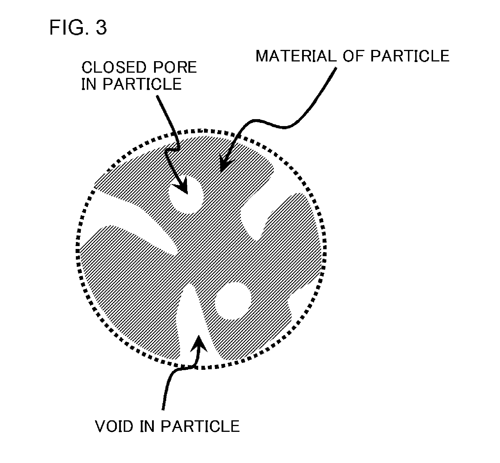
(Preparing Secondary Agglomerated Particles Configured of Primary Particles of Scaly Boron Nitride)

[0135]A mixture (melamine borate:scaly boron nitride powder=10:1 (mass ratio)) obtained by mixing melamine borate (borate:melamine=2:1 (molar ratio)) and scaly boron nitride powder (average major diameter: 15 μm) is added to a 0.2 mass % polyacrylic acid ammonium aqueous solution and is mixed for two hours to prepare a slurry for spray drying granulation (polyacrylic acid ammonium aqueous solution:mixture=100:30 (mass ratio)). Next, the slurry is supplied to a spray granulator and is sprayed under conditions of a number of rotations of an atomizer of 15000 rpm, a temperature of 200° C., and an amount ...


PUM

PropertyMeasurementUnit
porosityaaaaaaaaaa
pore diameteraaaaaaaaaa
average major diameteraaaaaaaaaa

Abstract

A thermally conductive sheet includes a thermosetting resin and an inorganic filler material dispersed in the thermosetting resin. Measuring a pore diameter distribution through mercury intrusion technique for the inorganic filler material included in an incineration residue after a cured product of the thermally conductive sheet is heated and incinerated at 700° C. for four hours, a porosity of the inorganic filler material represented as 100×b / a is greater than or equal to 40% and less than or equal to 65% given that a is the volume of particles of the inorganic filler material included in the incineration residue, and b is the volume of voids in the particles of the inorganic filler material included in the incineration residue. An average pore diameter of the inorganic filler material included in the incineration residue is greater than or equal to 0.20 μm and less than or equal to 1.35 μm.

Description

[0001]This application is based on Japanese patent application No. 2014-137235, the content of which is incorporated hereinto by reference.BACKGROUND[0002]1. Technical Field[0003]The present invention relates to a thermally conductive sheet, a cured product of the thermally conductive sheet, and a semiconductor device.[0004]2. Related Art[0005]It is known in the related art that an inverter device or a power semiconductor device is configured by mounting electronic components including a semiconductor chip such as an insulated gate bipolar transistor (IGBT) or a diode, a resistor, a capacitor, and the like on a substrate.[0006]These power control devices are applied to various devices depending on the breakdown voltage and the current capacity of the power control devices. Particularly, use of these power control devices is becoming widespread in various electrical machines in terms of recent environmental problems and promotion of saving energy.[0007]It is particularly desired for ...

Claims


Application Information

Patent Timeline
Patent Type & Authority Applications(United States)
IPC IPC(8): C08K7/24C08K3/38H01L23/29H01L23/495
CPCC08K7/24C08K3/38C08K2003/385H01L23/293H01L23/49568H01L2924/181H01L2224/32245H01L2224/48091H01L2224/48137H01L2224/48247H01L2224/73265H01L23/3737H01L23/4334H01L23/49575H01L23/295H01L23/3107H01L2924/00014H01L2924/00012H01L2924/00
Inventor MOCHIZUKI, SHUNSUKEKITAGAWA, KAZUYASHIRATO, YOJINAGAHASHI, KEITATSUDA, MIKAHIRASAWA, KAZUYAKUROKAWA, MOTOMI
Owner SUMITOMO BAKELITE CO LTD
Why Eureka
Try Eureka