

Titanium target for sputtering and manufacturing method thereof
a technology of titanium target and sputtering chamber, which is applied in the direction of electrolysis components, vacuum evaporation coatings, coatings, etc., can solve the problems of affecting the balance between the constituent substances prone to thinning and shortening of thin films used in semiconductor devices and the like, and affecting the stability of the subject film and the adjacent film, so as to effectively inhibit the generation of particles, stabilize the sputtering characteristics
- Summary
- Abstract
- Description
- Claims
- Application Information
AI Technical Summary
Benefits of technology
Problems solved by technology
Method used
Image

Examples
example 1
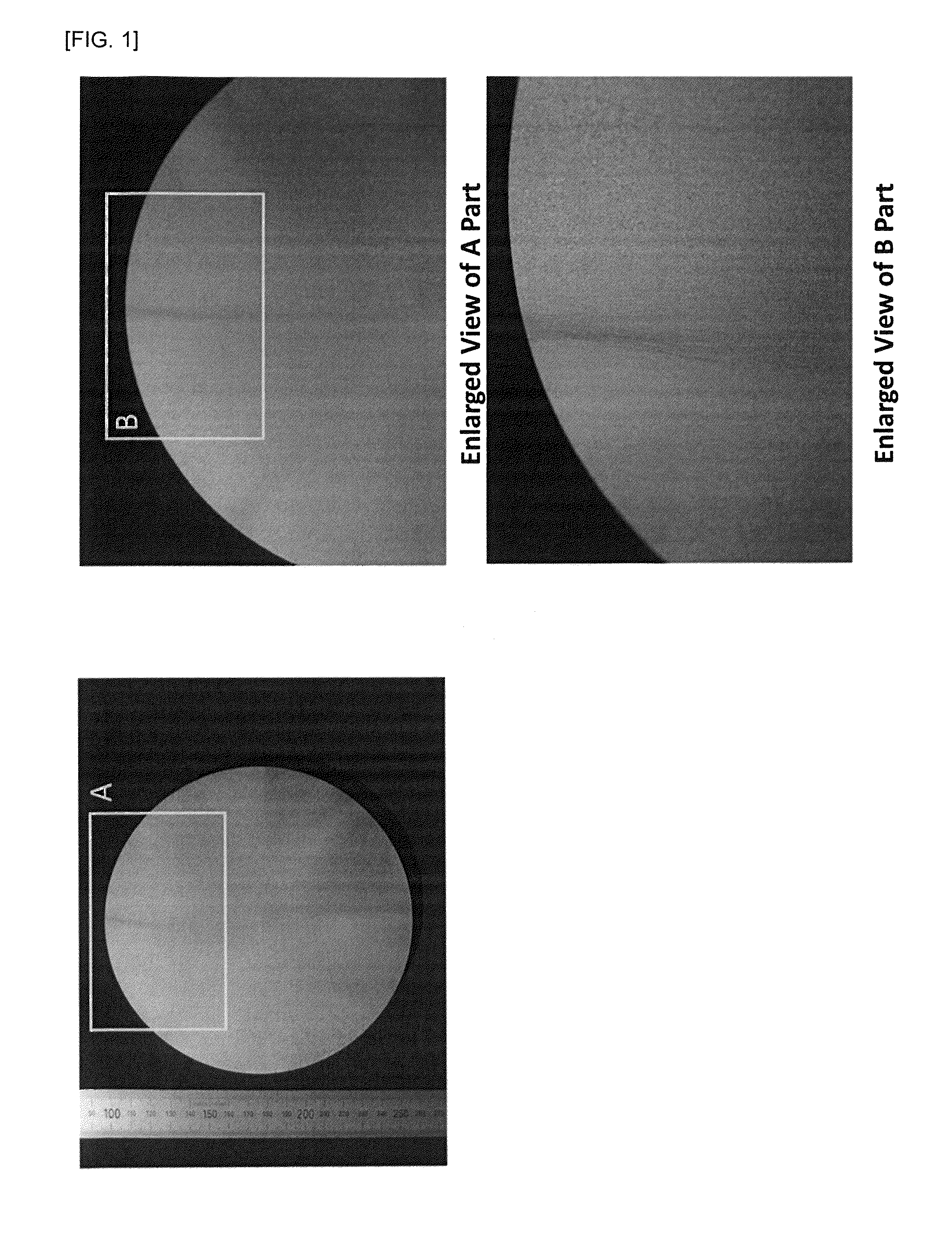
[0061]A titanium ingot obtained by melting and casting titanium having a purity of 5N5 was subject to primary forging at 850° C. and secondary forging at 600° C., subsequently cut and subject to cold rolling, and thereafter subject to heat treatment at 430° C. in a fluidized bed furnace. In addition, the resultant product was machined and diffusion-bonded with a Cu alloy backing plate to prepare a sputtering target having a titanium diameter of approximately φ430 mm.
[0062]The thus prepared titanium target was free from the macro pattern irregularity defined in the present invention, and the average crystal grain size was uniform in the plane; specifically, the average crystal grain sizes were respectively 8 μm at the center part, 9 μm at the R / 2 part, and 8 μm at the peripheral part. Note that R represents the radius of the disk-shaped target.
[0063]Note that the average crystal grain size was measured by observing the area of 190 μm×230 μm of the respective locations, and performing...
example 2
[0067]An ingot obtained by melting and casting titanium having a purity of 5N5 was subject to primary forging at 800° C. and compaction forging at 500° C., subsequently cut and subject to cold rolling, and thereafter subject to heat treatment at 460° C. in a fluidized bed furnace. In addition, the resultant product was machined and diffusion-bonded with a Cu alloy backing plate to prepare a sputtering target having a titanium diameter of approximately φ430 mm. The thus prepared titanium target was free from a macro pattern, and the average crystal grain size was uniform; specifically, the average crystal grain sizes were respectively 9 μm at the center part, 9 μm at the R / 2 part, and 9 μm at the peripheral part.
[0068]Moreover, the crystal orientation ratios were respectively 74% at the center part, 75% at the R / 2 part, and 73% at the peripheral part. Moreover, a TiN film having a thickness of 20 nm was formed on a SiO2 substrate at a power of 38 kW as a sputtering condition.
[0069]As...
reference example 2
[0074]An ingot obtained by melting and casting titanium having a purity of 5N5 was subject to primary forging at 800° C. and compaction forging at 500° C., subsequently cut and subject to cold rolling, and thereafter subject to heat treatment at 470° C. in a fluidized bed furnace. In addition, the resultant product was machined and diffusion-bonded with a Cu alloy backing plate to prepare a sputtering target having a titanium diameter of approximately φ430 mm.
[0075]The thus prepared titanium target was free from a macro pattern, but the average crystal grain size was larger than 10 μm; specifically, the average crystal grain sizes were respectively 12 μm at the center part, 13 μm at the R / 2 part, and 13 μm at the peripheral part. Moreover, the crystal orientation ratios were respectively 82% at the center part, 83% at the R / 2 part, and 80% at the peripheral part. Moreover, a TiN film having a thickness of 20 nm was formed on a SiO2 substrate at a power of 38 kW as a sputtering condi...
PUM
| Property | Measurement | Unit |
|---|---|---|
| crystal grain size | aaaaa | aaaaa |
| temperature | aaaaa | aaaaa |
| temperature | aaaaa | aaaaa |
Abstract
Description
Claims
Application Information