Reusable nitride wafer, method of making, and use thereof

a nitride wafer and reusable technology, applied in the direction of crystal growth process, natural mineral layer products, semiconductor lasers, etc., can solve the problems of affecting the quality and reliability of these devices, affecting the growth of epitaxial layers, and affecting the yield of secondary electrons, so as to achieve the effect of high secondary electron yield

Active Publication Date: 2016-01-21
SLT TECH
View PDF5 Cites 44 Cited by
  • Summary
  • Abstract
  • Description
  • Claims
  • Application Information

AI Technical Summary

Benefits of technology

[0010]In one embodiment, gallium-containing nitride wafers are disclosed, comprising a crystalline substrate member having a diameter greater than about 25 millimeters; a substantially wurtzite structure; a first, epi-ready, large-area surface, characterized by a root-mean-square surface roughness less than about 0.5 nanometer measured over an area of 20 micrometers by 20 micrometers, a surface threading density less than about 107 cm−2, a stacking-fault concentration below about 102 cm−1, and a symmetric x-ray rocking curve full width at half maximum (FWHM) less than about 100 arcsec; a second large-area surface, characterized by a root-mean-square surface roughness less than about 10 micrometers measured over an area of at least 20 micrometers by 20 micrometers; an edge perimeter that is substantially round, with at least one orientation flat; and at least one regrowth interface, wherein the at least one regrowth interface is substantially parallel to the first, epi-ready surface; an average concentration of at least one impurity selected from oxygen, hydrogen, silicon, carbon, fluorine, chlorine, lithium, sodium, and potassium, in a five-micrometer-thick layer on one side of the at least one regrowth interface is higher than an average concentration of the impurity in a five-micrometer-thick layer on an opposite side of the at least one regrowth interface by at least at least five percent and by less than a factor of five; and an average concentration of at least one impurity within a 5 micrometer-thick layer centered at the at least one regrowth interface is greater than an average concentration of the impurity in a five-micrometer-thick layer on opposite sides of the at least one regrowth interface by at least 10 percent and by less than a factor of 103.
[0011]In another embodiment, a bulk single-crystal semiconductor wafer is disclosed, comprising: (a) a crystalline substrate member having a thickness between about 100 micrometers and about 10 millimeters, a first surface being epi-ready, and first, second and third layers having first, second and third average impurity concentrations, respectively, wherein the second average impurity concentration is less than the third average impurity concentration, and the first average impurity concentration is greater than both the second and third average impurity concentrations; (b) at least one regrowth interface within the first layer, the regrowth interface being substantially parallel to the first surface and separated from the first surface by a distance of at least 10 micrometers, the regrowth interface having a secondary electron yield higher than that of the material immediately above and below the regrowth interface; (c) the wafer being heatable to at least 950° C. for six hours in an atmosphere consisting essentially of ammonia at a pressure of about 760 Torr without undergoing visible degradation
[0012]In yet another embodiment, a reusable bulk GaN single-crystal semiconductor wafer is disclosed, comprising: (a) a first layer having a first average impurity concentration; (b) a regrowth interface within the first layer, wherein the regrowth interface has a higher secondary electron yield than that of the material immediately above and below the interface; (c) a second layer having a second average impurity concentration; (d) a third layer having a third average impurity concentration, the first layer lying between the second layer and the third layer; wherein the second average impurity concentration is within a first range of the third average impurity concentration and the first average impurity concentration is within a second range of both the second and third average impurity concentrations.

Problems solved by technology

The quality and reliability of these devices, however, is compromised by high defect levels, particularly threading dislocations, grain boundaries, and strain in semiconductor layers of the devices.
Additional defects can arise from thermal expansion mismatch, impurities, and tilt boundaries, depending on the details of the growth of the layers.
The presence of defects has a deleterious effect on epitaxially-grown layers.
Such effect includes compromising electronic device performance.
To overcome these defects, techniques have been proposed that require complex, tedious fabrication processes to reduce the concentration and / or impact of the defects.
While a substantial number of conventional growth methods for gallium nitride crystals have been proposed, limitations still exist.
Bow, stress, and strain can cause low yields when slicing the boules into wafers, and can make the wafers susceptible to cracking during downstream processing, and may also negatively impact device reliability and lifetime.
Most large area substrates are manufactured by vapor-phase methods such as hydride vapor phase epitaxy (HVPE), which are relatively expensive.
However, ammonothermal manufacturing capabilities remain limited and substrate costs to date are higher than HVPE.
However, flux manufacturing capabilities remain very limited and GaN substrates synthesized by flux methods are not yet available commercially.

Method used


Image

  • Reusable nitride wafer, method of making, and use thereof
  • Reusable nitride wafer, method of making, and use thereof
  • Reusable nitride wafer, method of making, and use thereof

Examples


example 1

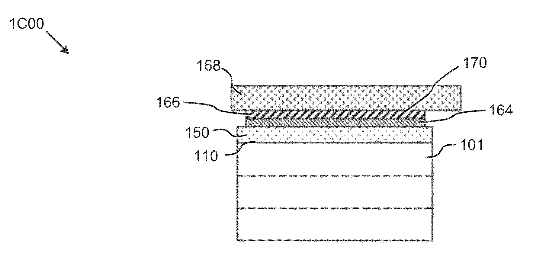
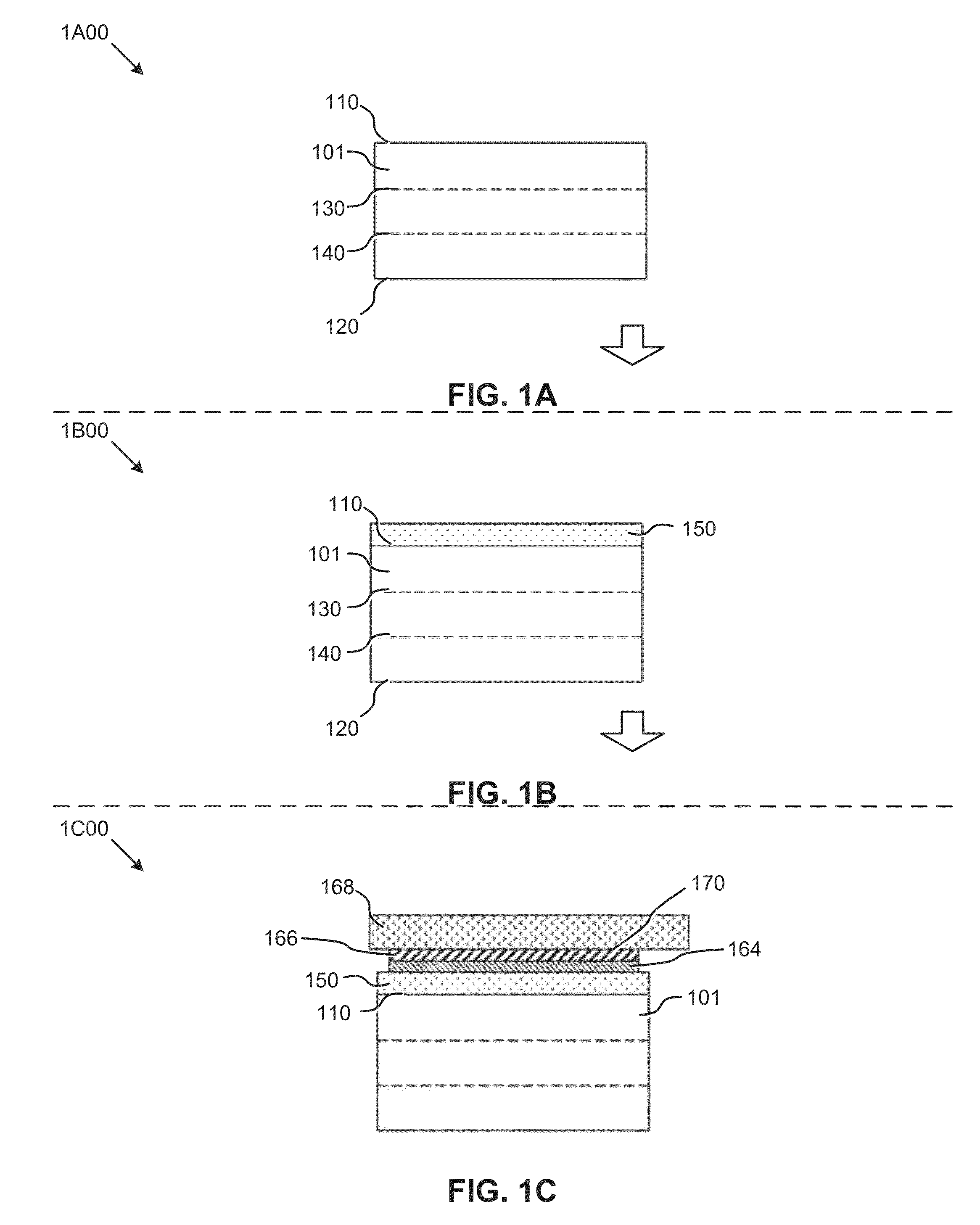
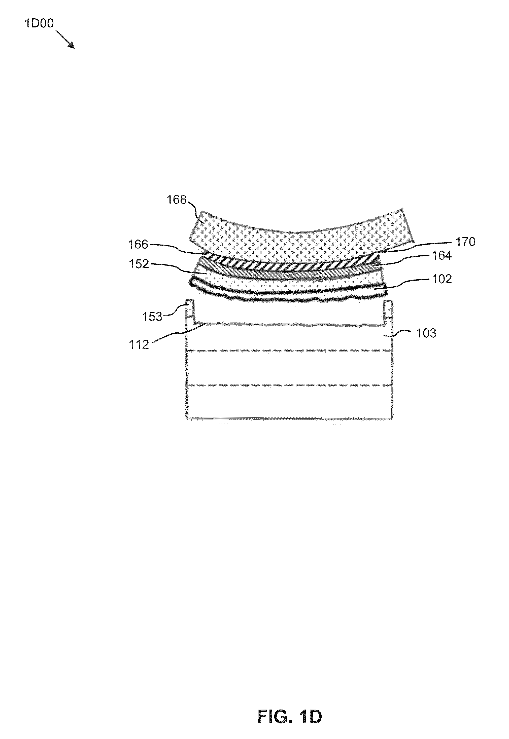
[0046]An epitaxial LED device layer, comprising an n-type layer, an InGaN active layer, and a p-type later, is deposited on an HVPE-grown wafer by MOCVD, with a total thickness of approximately 4 micrometers. A nickel-based stressor layer is deposited overlying the device layer, and a flexible handle layer is cemented onto the stressor layer. A vertical load is applied to the flexible handle layer, causing spalling of the epitaxial LED device layer plus approximately 40 micrometers of the original substrate.

[0047]The spalled wafer is broken into two pieces. For the first of the two pieces, the spalled surface of the GaN wafer is lapped, polished, dry-etched, and chemical-mechanically polished, while the second half-wafer is left in the as-spalled condition. Both pieces are then fastened to a rigid seed rack and inserted into a silver capsule along with a 13.4% open area baffle, polycrystalline GaN nutrient, NH4F mineralizer, and ammonia, and the capsule is sealed. The ratios of GaN ...


PUM

PropertyMeasurementUnit
thicknessaaaaaaaaaa
thicknessaaaaaaaaaa
thicknessaaaaaaaaaa

Abstract

Techniques for processing materials for manufacture of gallium-containing nitride substrates are disclosed. More specifically, techniques for fabricating and reusing large area substrates using a combination of processing techniques are disclosed. The methods can be applied to fabricating substrates of GaN, AlN, InN, InGaN, AlGaN, and AlInGaN, and others. Such substrates can be used for a variety of applications including optoelectronic devices, lasers, light emitting diodes, solar cells, photo electrochemical water splitting and hydrogen generation, photo detectors, integrated circuits, transistors, and others.

Description

REFERENCE TO RELATED APPLICATION[0001]This application claims priority to Provisional Application No. 62 / 026,777, filed Jul. 21, 2014, hereby incorporated by reference.FIELD[0002]This disclosure relates generally to techniques for processing materials for manufacture of gallium-containing nitride substrates. More specifically, embodiments of the disclosure include techniques for fabricating and reusing large area substrates using a combination of processing techniques.BACKGROUND[0003]Gallium nitride (GaN)-based optoelectronic and electronic devices are of tremendous commercial importance. The quality and reliability of these devices, however, is compromised by high defect levels, particularly threading dislocations, grain boundaries, and strain in semiconductor layers of the devices. Threading dislocations can arise from a lattice mismatch of GaN-based semiconductor layers to a non-GaN substrate such as sapphire or silicon carbide. Grain boundaries can arise from the coalescence fro...

Claims


Application Information

Patent Timeline
Patent Type & Authority Applications(United States)
IPC IPC(8): H01L29/20H01L29/04H01L29/36
CPCH01L29/2003H01L29/36H01L29/045H01L29/04H01L21/7813H01L33/32Y02E10/544H01L31/1856H01L31/1892H01L33/0093H01L31/00C30B23/025C30B25/18C30B29/406H01L21/0254H01L31/03044H01L33/0075H01S5/3013
Inventor D'EVELYN, MARK P.KRAMES, MICHAEL RAGAN
Owner SLT TECH
Why Eureka
Try Eureka