Short-Gate Tunneling Field Effect Transistor Having Non-Uniformly Doped Vertical Channel and Fabrication Method Thereof

a field effect transistor and vertical channel technology, applied in the direction of semiconductor devices, diodes, electrical apparatus, etc., can solve the problems of transistor performance degradation, achieve the effect of enhancing the gate control ability of the transistor, steeper sub-threshold slope, and tunneling width

Inactive Publication Date: 2016-01-21
PEKING UNIV
View PDF14 Cites 14 Cited by
  • Summary
  • Abstract
  • Description
  • Claims
  • Application Information

AI Technical Summary

Benefits of technology

[0024]1. Owing to the vertical channel design of the transistor, a double-gate structure of the control gates is easily achieved in the process, and thus the gate control ability of the transistor is enhanced so that an on-current of the transistor is increased and a steeper sub-threshold slope is obtained.
[0025]2. Because of the non-uniform doping design of the channel, the doping concentration in the channel near the drain region is relatively higher, so that an electrical field at the drain region cannot penetrate through and reach the tunneling junction at the source region, and thus an impact of the drain voltage on the tunneling width of the tunneling junction at the source region is effectively reduced and the super exponential relationship between the output tunneling current and the drain voltage is weakened, and consequently the output resistance is reduced and the output characteristic of the transistor is improved.
[0026]3. Attributing to the short-gate design of the transistor, the gate underlapped region of the channel near the drain region forms a high resistance region, so that during an increase of the drain voltage, the drain voltage will mostly drop at the gate underlapped region, and thus the impact of the drain voltage on the tunneling width of the tunneling junction at the source region is effectively reduced, and in turn the output characteristic of the transistor is improved.
[0027]4. Since the transistor has a gate overlapped region in the source region, a tunneling perpendicular to a surface of the gate will occur in the gate overlapped source region, and thus a tunneling area is increased and the on-current of the transistor is increased.
[0028]5. By means of the L-shape structure of the control gates of the transistor, an intensity of the electrical field at corners of the control gates are large, which increases a tunneling electric field of the tunneling junction at the source region and thus it is beneficial to increase the on-current of the transistor and to gain a steeper sub-threshold slope.
[0029]Compared with the conventional TFET, the short-gate tunneling field effect transistor having the non-uniformly doped vertical channel, by virtue of the structure design of the transistor, can effectively suppress the impact of the electrical field at the drain region on the tunneling width of the tunneling junction at the source region; the super exponential relationship between the output tunneling current and the drain voltage is weakened; and the output characteristic of the transistor is improved. Meanwhile, the tunneling field effect transistor is beneficial to increase the on-current of the transistor and to gain a steeper sub-threshold slope.

Problems solved by technology

Since an excessively short length of the gate underlapped region cannot produce the effect of dramatically improving the output characteristic of the TFET, and an excessively long length of the gate underlapped region may weaken the gate control for the entire channel of the transistor and thus result in a degradation in the performance of the transistor, the length of the gate underlapped region is generally optimized as 50% or more of the length of the entire channel (i.e., the length between a edge of the source region and an edge of the drain region).

Method used


Image

  • Short-Gate Tunneling Field Effect Transistor Having Non-Uniformly Doped Vertical Channel and Fabrication Method Thereof
  • Short-Gate Tunneling Field Effect Transistor Having Non-Uniformly Doped Vertical Channel and Fabrication Method Thereof
  • Short-Gate Tunneling Field Effect Transistor Having Non-Uniformly Doped Vertical Channel and Fabrication Method Thereof

Examples


Embodiment Construction

[0037]Hereinafter, the present invention will be described in detail in conjunction with embodiments. It should be noted that, embodiments are disclosed to help further understand the present invention. Those skilled in the art can appreciate that, various modifications and substitutions are possible without departing from the spirit and scope of the appended claims and the present invention. Therefore, the present invention should not be limited to the contents of the disclosed embodiments, and the scope of the present invention should be defined by the claims.

[0038]An implementation method for fabricating a short-gate tunneling field effect transistor having a non-uniformly doped vertical channel of the present invention will be further described below in detail by specific embodiments in conjunction with the attached drawings.

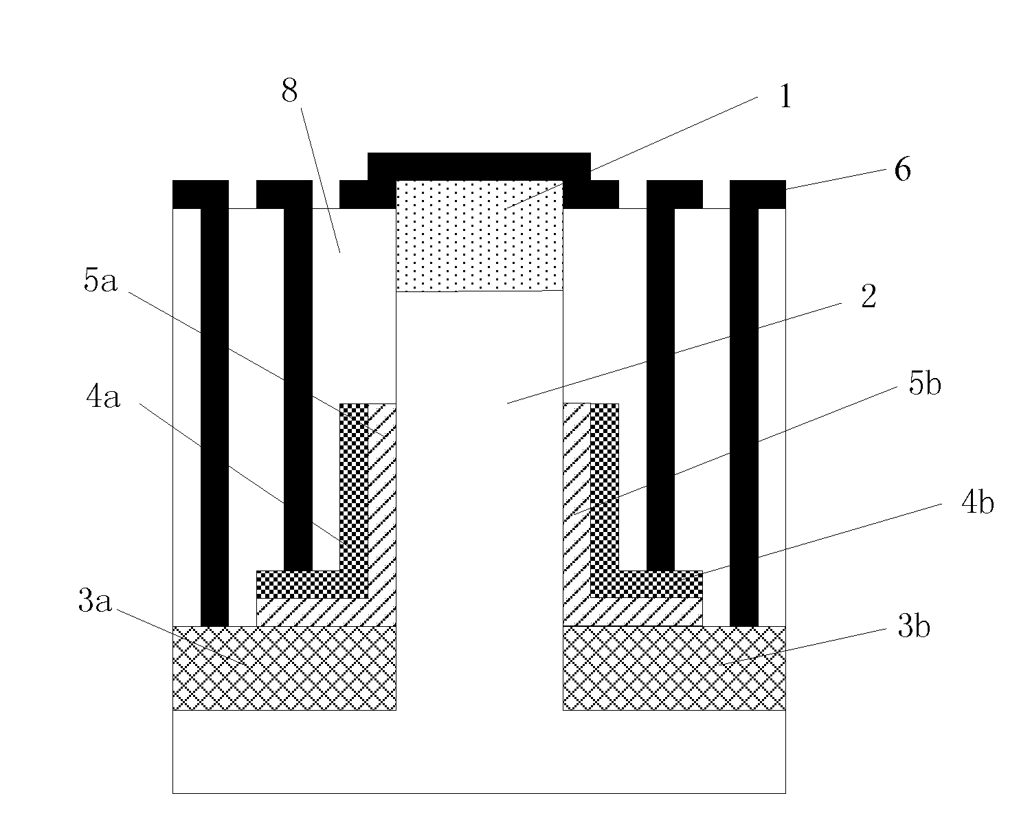
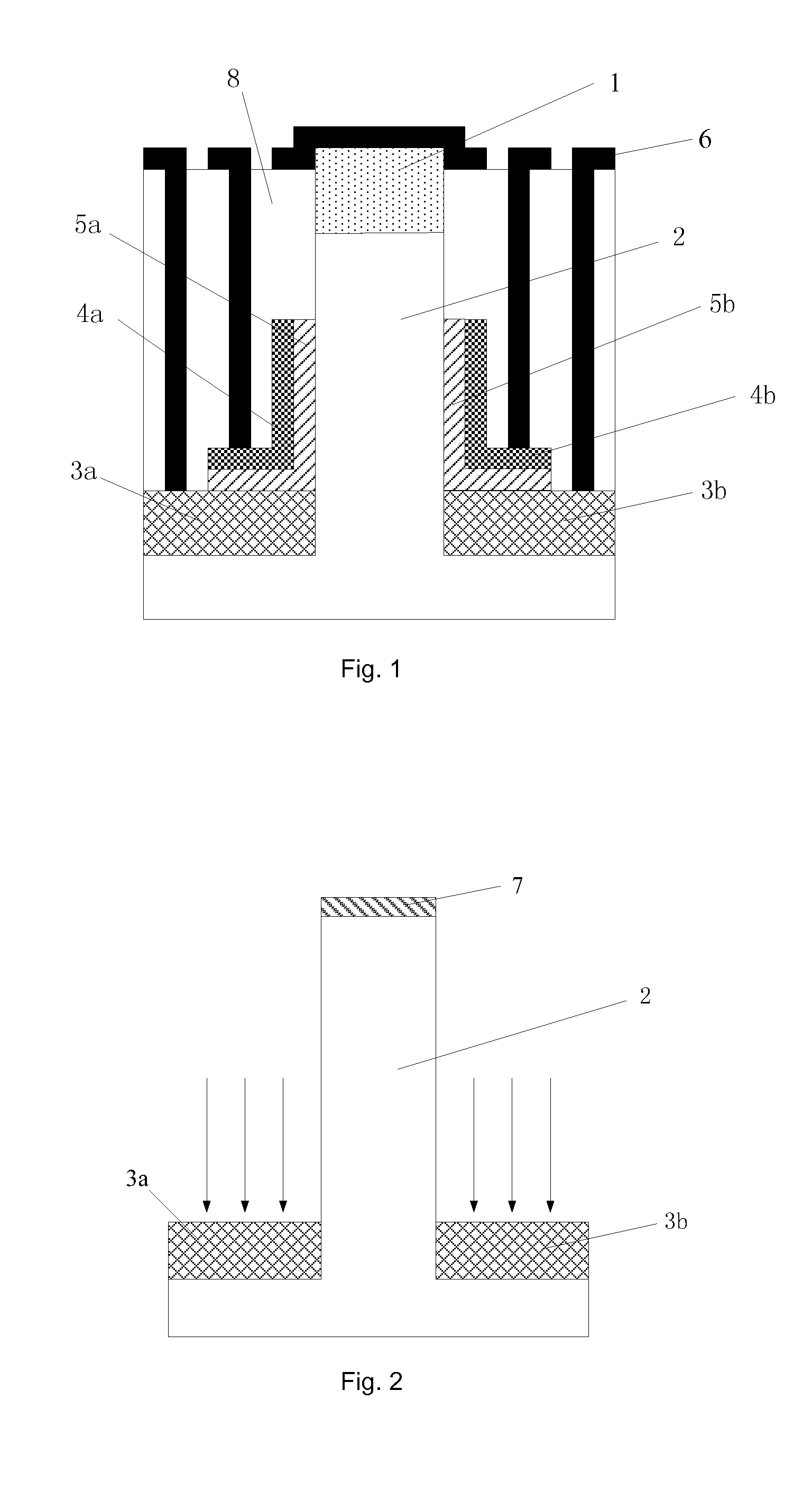
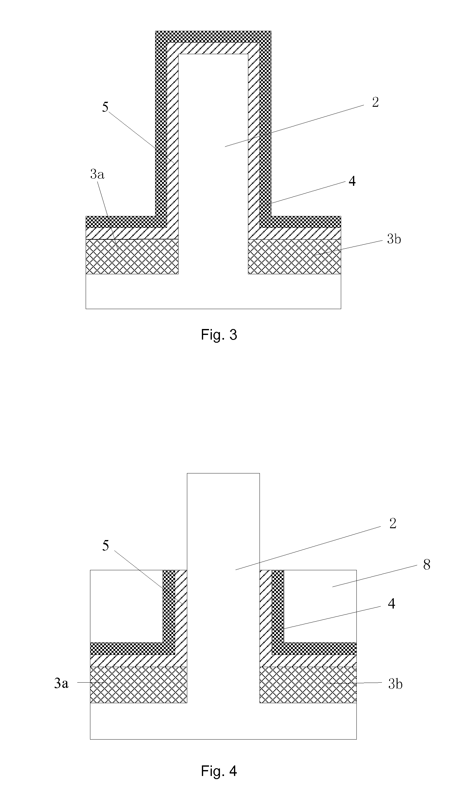
[0039]The specific implementation steps are shown in FIG. 2 to FIG. 6 (taking an N-type transistor as an example).

[0040]1. A Si3N4 film is deposited on a se...


PUM


Abstract

The present invention discloses a short-gate tunneling field effect transistor having a non-uniformly doped vertical channel and a fabrication method thereof. The short-gate tunneling field effect transistor has a vertical channel and the channel region is doped in such a slowly-varied and non-uniform manner that a doping concentration in the channel region appears a Gaussian distribution along a vertical direction and the doping concentration in the channel near the drain region is higher while the doping concentration in the channel near the source region is lower; and double control gates are formed at both sides of the vertical channel and the control gates form an L-shaped short-gate structure, so that a gate underlapped region is formed in the channel near the drain region, and a gate overlapped region is formed at the source region. As compared with a conventional TFET, the short-gate tunneling field effect transistor according to the present invention can effectively suppress the impact of the electrical field at the drain region on the tunneling width of the tunneling junction at the source region; the super exponential relationship between the output tunneling current and the drain voltage is weakened; and the output characteristic of the transistor is significantly improved. Meanwhile, the tunneling field effect transistor is beneficial to increase the on-current of the transistor and to gain a steeper sub-threshold slope.

Description

FIELD OF THE INVENTION[0001]The present invention relates to a field effect transistor logic device in CMOS ultra large scaled integrated (ULSI) circuits, and particularly relates to a short-gate tunneling field effect transistor having a non-uniformly doped vertical channel.BACKGROUND OF THE INVENTION[0002]Since the birth of the first integrated circuit, the technology of the integrated circuit has been developing following the Moore's law all the time. The semiconductor device has been sized down continuously. Meanwhile, because a sub-threshold slope of the conventional MOSFET cannot be decreased simultaneously with the shrink of the device due to the limitation of the thermoelectric force kT / q, a leakage current of the device increases, and thus the power consumption of the entire chip constantly rises, increasing the power consumption density of the chip sharply and thus severely blocking the chip from being applied to the system integration. In order to adapt to the developing ...

Claims


Application Information

Patent Timeline
Patent Type & Authority Applications(United States)
IPC IPC(8): H01L29/66H01L21/266H01L21/28H01L29/06H01L29/08H01L29/10H01L29/16H01L29/161H01L29/20H01L29/423H01L29/49H01L29/51H01L29/78
CPCH01L29/66977H01L29/0649H01L29/7831H01L29/42376H01L29/0847H01L29/1041H01L29/66666H01L29/66484H01L21/266H01L21/28194H01L21/28202H01L29/51H01L29/518H01L29/4916H01L29/495H01L29/16H01L29/161H01L29/20H01L29/7827B82Y10/00H01L29/0676H01L29/401H01L29/413H01L29/41775H01L29/66356H01L29/66439H01L29/7391
Inventor HUANG, RUWU, CHUNLEIHUANG, QIANQIANWANG, CHAOWANG, JIAXINWANG, YANGYUAN
Owner PEKING UNIV
Why Eureka
Try Eureka