Color Display Device Structure

a color display device and display device technology, applied in the field of display technology, can solve the problems of low productivity, high cost, only applicable to organic small molecules easily sublimated, etc., and achieve the effects of reducing the thickness of the light emitting layer and the thickness of the color display device, good emitting efficiency, and high color purity

Active Publication Date: 2016-01-28
SHENZHEN CHINA STAR OPTOELECTRONICS TECH CO LTD
View PDF0 Cites 20 Cited by
  • Summary
  • Abstract
  • Description
  • Claims
  • Application Information

AI Technical Summary

Benefits of technology

[0024]The color display device structure of the present invention, by the blue and green light emitting layer and the color conversion layer including the blue filter unit, the green filter unit and the red conversion unit, achieves color display and reduces the thickness of the light emitting layer and the thickness of the color display device. The material of the blue and green light emitting layer and the color conversion layer may be

Problems solved by technology

This technique is only applicable to organic small molecules material easily sublimated.
However, because of the need for high accuracy and precision of the mask alignment in the preparation of high-resolution display, it results in low productivity and high cost, and because of the life of the three primary colors, the excitation rate, and the large attenuation difference, it results in a color cast of the color display device.
However, since most of the light energy is absorbed

Method used


Image

  • Color Display Device Structure
  • Color Display Device Structure
  • Color Display Device Structure

Examples


first embodiment

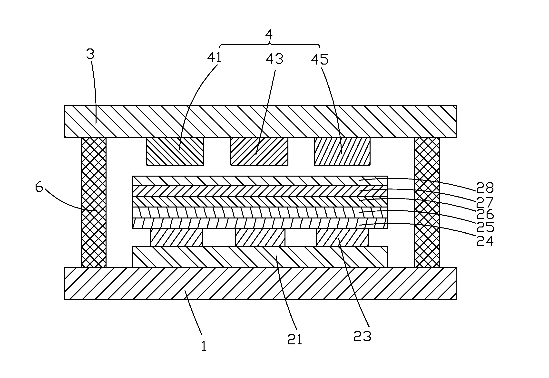
[0035]Please refer to FIG. 1. FIG. 1 is a schematic diagram of the color display device structure according to the present invention. The color display device structure includes a substrate 1, an anode 21 formed on the substrate 1, a thin film transistor (Thin Film Transistor, TFT) array 23 formed on the anode 21, a hole injection layer 24 (Hole Injection Layer, HIL) formed on the thin film transistor array 23, a hole transport layer (Hole Transport Layer, HTL) 25 formed on the hole injection layer 24, a light emitting layer 26 formed on the hole transport layer 25, an electron transport layer 27 (Electron Transport Layer, ETL) formed on the light emitting layer 26, a cathode 28 formed on the electron transport layer 27, a cover plate 3 set above the cathode 28 and bonded to the substrate 1, a color conversion layer 4 formed on the inner side of the cover plate 3, and a sealant 6 used to encapsulate the substrate 1 and the cover plate 3.

[0036]The light emitting layer 26 is a blue an...

second embodiment

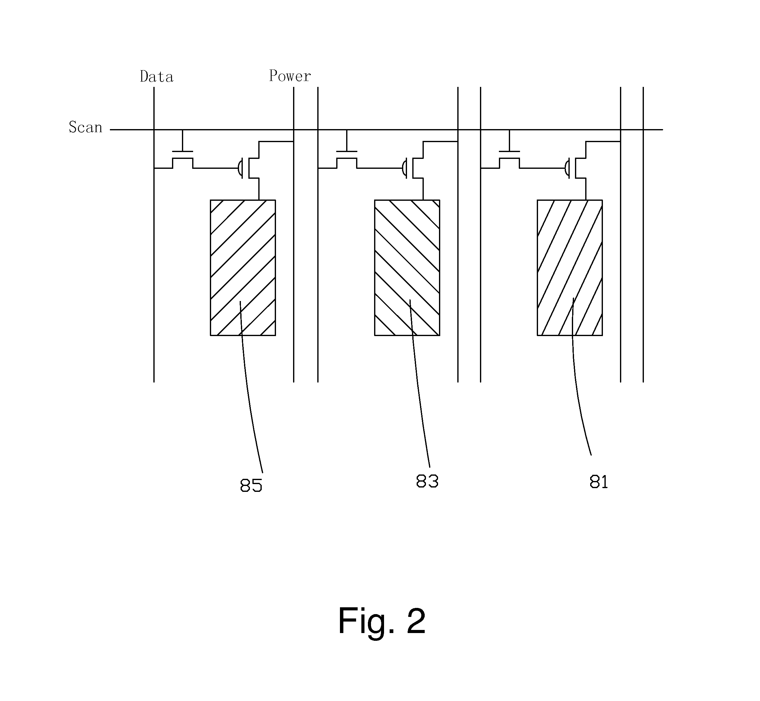
[0058]See FIG. 6. In the second embodiment, the blue filter unit 41, the green filter unit 43, the red conversion unit 45 and the white converting unit 47 correspond to a pixel. The pixel includes a red sub-pixel 85, a green sub-pixel 83, a blue sub-pixel 81 and a white sub-pixel 87. The red conversion unit 45 corresponds to the red sub-pixel 85 of the pixel. The green filter unit 43 corresponds to the green sub-pixel 83 of the pixel. The blue filter unit 41 corresponds to the blue sub-pixel 81 of the pixel. The white conversion unit 47 corresponds to the white sub-pixel 87 of the pixel. The red sub-pixel 85, the green sub-pixel 83, the blue sub-pixel 81 and the white sub-pixel 87, each corresponds to a TFT, to control whether the regions of the blue and green light emitting layer 26, respectively corresponding to the sub-pixels emit light or not.

[0059]See FIG. 7. In the second embodiment, the arranged ways of the upper and lower pixel lines adjacent to each are the same. The red su...


PUM


Abstract

The invention provides a color display device structure, including a substrate (1), an anode (21), a thin film transistor array (23), a hole injection layer (24), a hole transport layer (25), a light emitting layer (26), an electron transport layer (27), a cathode (28), a cover plate (3), a color conversion layer (4) formed on the inner side of the cover plate (3), and a sealant (6). The light emitting layer (26) is a blue and green light emitting layer (26). The color conversion layer (4) includes a blue filter unit (41), a green filter unit (43) and a red conversion unit (45) separated one another. The blue light and the green light emitted by the blue and green light emitting layer (26) is filtered to become blue light by the blue filter unit (41). The blue light and the green light emitted by the blue and green light emitting layer (26) is filtered to become green light by the green filter unit (43). The blue light and the green light emitted by the blue and green light emitting layer (26) is converted to red light by the red conversion unit (45). The color display is achieved by the color display device structure. The color display device structure is manufactured by a simple production process, and has the features of high color purity, good emitting efficiency, high stability, ultra-thin, and so on.

Description

BACKGROUND OF THE INVENTION[0001]1. Field of the Invention[0002]The present invention relates to the field of display technology, and more particularly, to a color display device structure and manufacturing method thereof.[0003]2. Description of Related Art[0004]The organic light emitting diode display (Organic Light Emitting Diode, OLED) is a very promising flat panel display technology, which not only has a very excellent display performance, but also has self-luminous, simple structure, ultra-thin, fast response, wide viewing angle, low power consumption, flexible display and other features, known as the “Dream monitor”. To be coupled with the investment of OLED in production equipment is much smaller than that of the liquid crystal display (Liquid Crystal Display, LCD), OLED has got the attention of the major display manufacturers and become the main force of third-generation display.[0005]Currently, there are several color OLED technology roadmap. One is RGB (Red, Green, Blue, ...

Claims


Application Information

Patent Timeline
IPC IPC(8): H01L27/32H01L51/50H01L51/52
CPCH01L51/5237H01L51/5036H01L27/1214H01L27/3262H01L51/5024H01L27/3244H01L27/3213H01L51/5246H01L27/322H10K59/38H10K50/115H10K50/125H10K2102/331H10K50/12H10K50/84H10K50/8426H10K59/12H10K59/351H10K59/1213
Inventor LIU, YAWEIWANG, YIFANLO, CHANGCHENG
Owner SHENZHEN CHINA STAR OPTOELECTRONICS TECH CO LTD
Why Eureka
Try Eureka