
Organic semiconductor compound thin film, method of fabricating the same and electronic device using the same

a technology of organic semiconductors and compound films, applied in semiconductor devices, solid-state devices, thermoelectric devices, etc., can solve the problems of determining the performance of various organic material-based electronic devices, and various methods that have different limits in solving fundamentally low electric charge mobility of conjugated polymers, so as to facilitate the formation of stack structures and improve lateral and vertical electric charge mobility.

Inactive Publication Date: 2016-02-04
GWANGJU INST OF SCI & TECH
View PDF5 Cites 2 Cited by
  • Summary
  • Abstract
  • Description
  • Claims
  • Application Information

AI Technical Summary

Benefits of technology

The present invention provides an organic semiconductor compound thin film that can be used on flexible substrates and exhibits high electric charge mobility. Additionally, the thin film is resistant to interlayer solvents, making it easy to form stack structures using a wet process. The resulting organic electronic device has improved lateral and vertical electric charge mobility.

Problems solved by technology

A major limiting factor for determining performance of various organic material-based electronic devices is low electric charge mobility of the conjugated polymers.
However, such methods have various limits in solving fundamentally low electric charge mobility of the conjugated polymer.
However, since the conjugated polymers make three-dimensional (3-D) interaction with each other during change into a solid thin film, that is, a large number of amorphous regions and defect sites are generated during alignment of the conjugated polymers from side to side or from top to bottom, the conjugated polymers finally exhibit low charge carrier mobility in a device.
However, induction of crystallinity only to the substrate surface is insufficient to induce overall crystallinity of the thin film through a total thickness (about 70 nm to about 80 nm) thereof.

Method used


Image

  • Organic semiconductor compound thin film, method of fabricating the same and electronic device using the same
  • Organic semiconductor compound thin film, method of fabricating the same and electronic device using the same
  • Organic semiconductor compound thin film, method of fabricating the same and electronic device using the same

Examples


experimental example 1

[0088]In each of four glass vials, 10 mg of P3HT as a conjugated polymer and 1 ml of chloroform were placed, followed by stirring at room temperature for 1 hour.

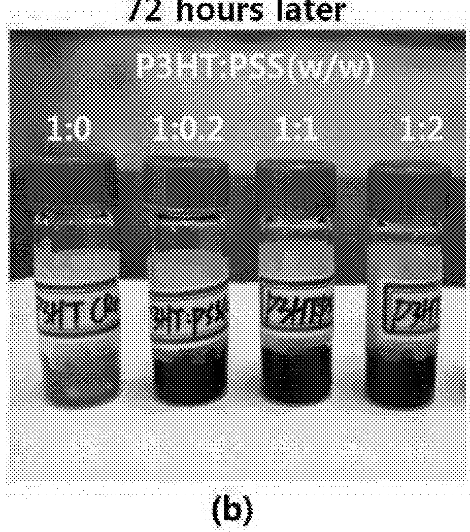
[0089]Next, 0 mg, 11 mg, 55 mg, and 111 mg of PSS (18% by weight (wt %) in water) were placed in the four glass vials, respectively, followed by stirring at room temperature for about 72 hours. Here, weight ratios of P3HT to PSS were 1:0, 1:0.2, 1:1, and 1:2, respectively.

[0090]Next, the solutions prepared in this way were coated onto a substrate to form P3HT and P3HT:PSS thin films having a thickness from about 70 nm to about 100 nm

[0091]FIG. 3 shows images of crystal seeds formed in dispersions obtained by adding PSS to P3HT.

[0092]In FIG. 3, changes occurring between P3HT and PSS over time are shown.

[0093]FIG. 3(a) shows an image of dispersions as-prepared by adding PSS to a P3HT solution in weight ratios of P3HT to PSS of 1:0, 1:0.2, 1:1 and 1:2, respectively, and FIG. 3(b) shows an image of the dispersions of FIG. 3(a) a...

experimental example 2

[0122]OFET devices using solutions obtained by adding PSS to various conjugated polymers and stirring these materials were analyzed. In this experiment, a conjugated polymer thin film or a conjugated polymer:PSS thin film was formed as a semiconductor layer on a Si / Si02 substrate, followed by forming a gate electrode (G) at a lower side of the

[0123]Si / Si02 substrate. Next, a source electrode (S) and a drain electrode (D) were formed to be separated from each other on the conjugated polymer thin film or the conjugated polymer:PSS thin film, thereby preparing an OFET device (L=50 μm, W=1000 μm). Here, a region of the semiconductor layer between the source electrode (S) and the drain electrode (D) corresponds to an active layer channel.

[0124]FIG. 10(a) shows transfer curves depicting characteristics of the OFET devices using P3HT and P3HT:PSS thin films, respectively.

[0125]FIG. 10(b) shows transfer curves depicting characteristics of the OFET devices using PDVT-10 and PDVT-10:PSS thin ...

experimental example 3

[0141]An organic solar cell using a P3HT:PSS thin film according to one embodiment of the present invention was prepared, followed by analyzing characteristics thereof.

[0142]FIG. 14 is a schematic diagram of an organic solar cell using a P3HT:PSS thin film.

[0143]Referring to FIG. 14, a organic solar cell stack was prepared by sequentially stacking an ITO electrode, a PEDOT:PSS hole transporting layer, a photoactive layer and an aluminum electrode on a glass substrate.

[0144]Here, the photoactive layer has a bi-layer structure including an electron donor layer and an electron acceptor layer formed on the electron donor layer. Here, the electron to donor layer was prepared using a P3HT thin film or a P3HT:PSS thin film, and the electron acceptor layer was prepared using a PCMB thin film.

[0145]FIG. 15 shows graphs depicting characteristics of organic solar cells using P3HT and P3HT:PSS thin films, respectively.

[0146]Referring to FIG. 15, changes in performance of organic solar cell stac...


PUM

PropertyMeasurementUnit
thicknessaaaaaaaaaa
thicknessaaaaaaaaaa
domain sizeaaaaaaaaaa

Abstract

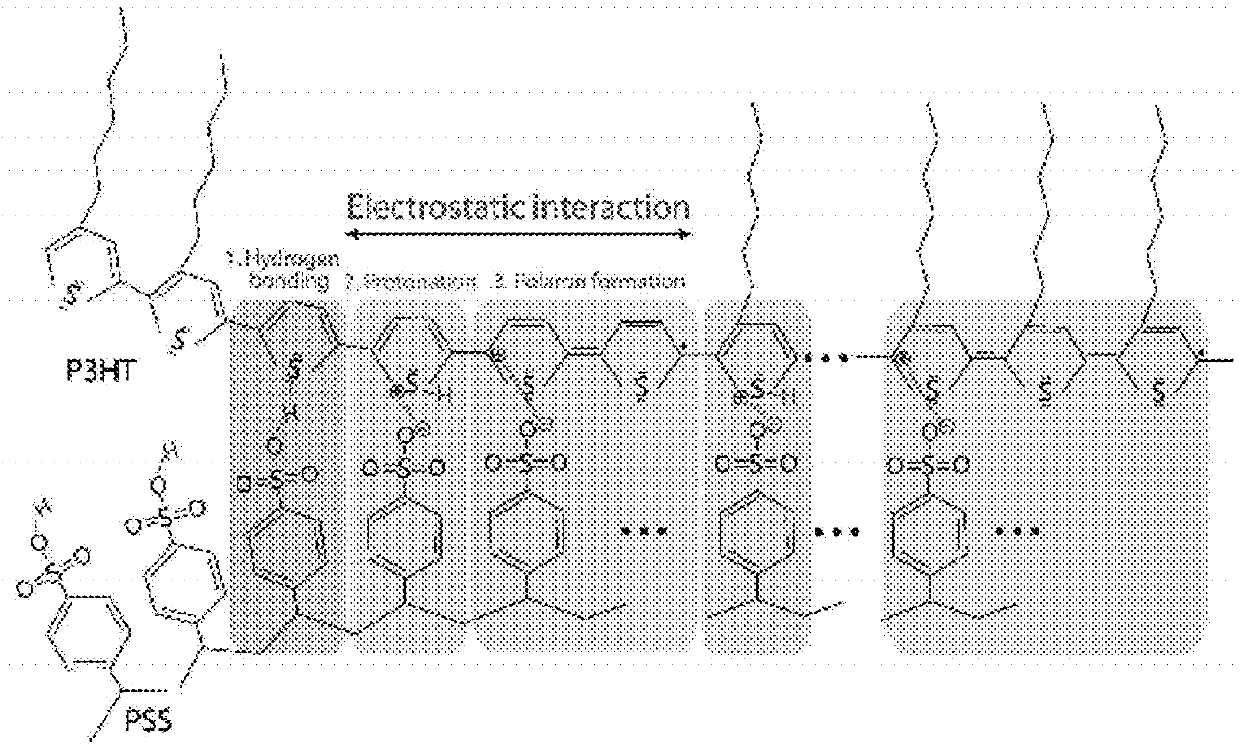
Disclosed herein is an organic semiconductor compound thin film. The organic semiconductor compound thin film includes a conjugated organic material including an unshared electron pair-containing sulfur or nitrogen atom and exhibiting semiconductivity, and a polymeric organic acid bonded to the conjugated organic material through hydrogen bonding and protonation. The organic semiconductor compound thin film exhibits high electric charge mobility and interlayer solvent resistance to facilitate formation of a stack structure despite use of a wet process.

Description

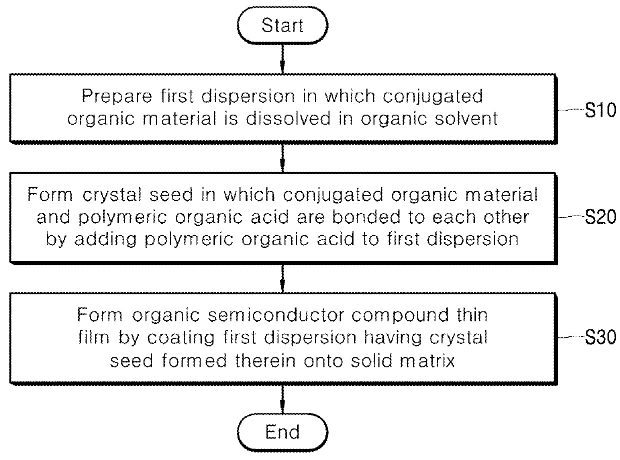
BACKGROUND[0001]1. Technical Field[0002]The present invention relates to an organic semiconductor compound thin film, a method of fabricating the same, and an electronic device using the same. More particularly, the present invention relates to an organic semiconductor compound thin film exhibiting high electric charge mobility by inducing crystallization of a conjugated organic material via an organic acid, a method of fabricating the same, and an electronic device using the same.[0003]2. Description of the Related Art[0004]Since an organic electronic device using a conjugated polymer has various merits such as low price, very easy manufacturing process, lightweight and bendability as compared with electronic devices based on inorganic materials such as silicon and the like, the organic electronic device using a conjugated polymer is spotlighted as a future energy source and is currently the focus of much research.[0005]To commercialize such an organic material-based electronic dev...

Claims


Application Information

Patent Timeline
Patent Type & Authority Applications(United States)
IPC IPC(8): C08L25/06H10K99/00C08L41/00
CPCH01L51/0036C08L41/00H01L51/42H01L51/0003H01L51/0512C08L25/06C08L25/18Y02E10/549C08G61/122C08G61/123C08G61/126C08G2261/1412C08G2261/3223C08G2261/3327C08G2261/334C08G2261/344C08G2261/364C08G2261/794C08G2261/91C08G2261/92H10K71/12H10K85/215H10K85/113H10K10/484H10K30/20H10K30/50C08L65/00C08J5/2256C08J5/18
Inventor LEE, KWANGHEEKWON, SOONCHEOLYU, KILHOKWEON, KYOUNG CHUN
Owner GWANGJU INST OF SCI & TECH
Learn More