

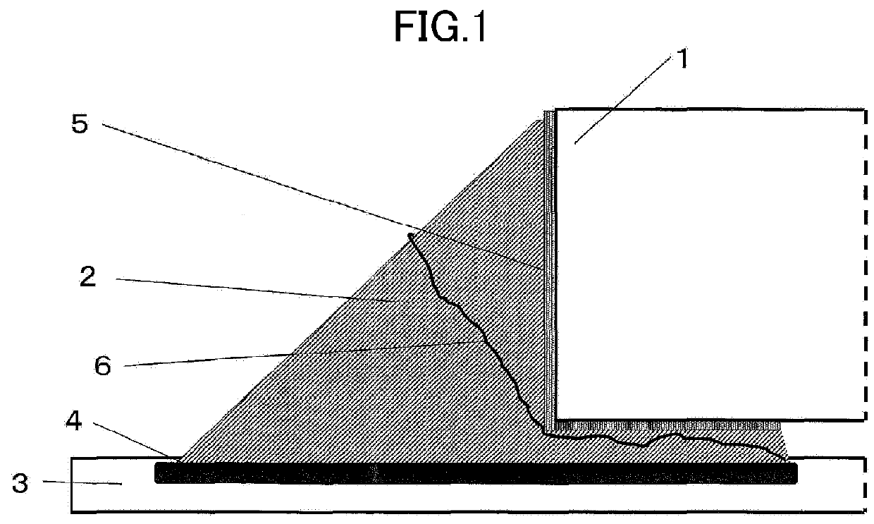
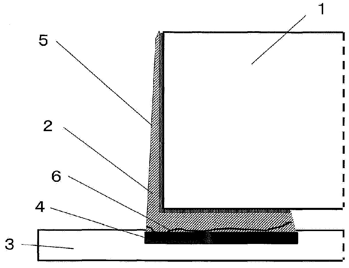
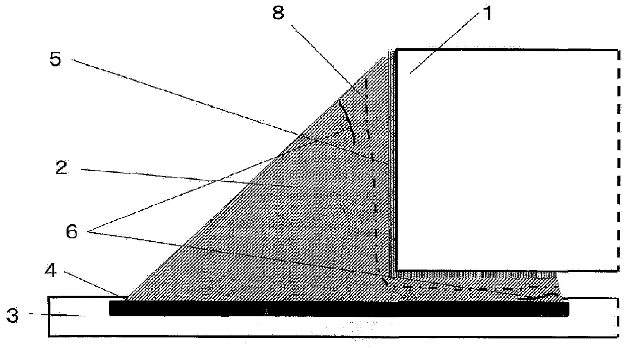
Lead-free solder alloy and in-vehicle electronic circuit
a technology of in-vehicle electronic circuit and solder alloy, which is applied in the direction of soldering apparatus, coupling device connection, manufacturing tools, etc., can solve the problems of thermal expansion and contraction, certain degree of thermal displacement, and severe operating environment, so as to suppress crack propagation, prevent the effect of propagation, and excellent temperature cycle characteristics
- Summary
- Abstract
- Description
- Claims
- Application Information
AI Technical Summary
Benefits of technology
Problems solved by technology
Method used
Image

Examples
example 1
[0052]In Table 1, the liquidus temperature, the SnSb particle size as the initial value and after 1,500 cycles in the temperature cycle test, and the crack ratio of the respective solder alloys in Table 1 were measured by the following methods.
(Solder Melting Test)
[0053]Each solder alloy in Table 1 was prepared to measure the solder melting temperature. The solidus temperature was measured by a method according to JIS Z3198-1. The liquidus temperature was measured not by applying JIS Z3198-1 but by the same DSC method as the method of measuring the solidus temperature according to JIS Z3198-1.
[0054]The results are shown in the column of “Liquidus temperature” in Table 1.
(Temperature Cycle Test)
[0055]Each solder alloy in Table 1 was atomized to form solder powder. The solder powder was mixed with soldering flux including pine resin, a solvent, an activator, a thixotropic agent, an organic acid and the like to prepare solder paste of each solder alloy. The solder paste was printed on ...
example 2
[0066]Next, in Table 2, the ratio of crack occurrence and the rate of residual shear strength after 3,000 cycles in the temperature cycle test were measured in the respective solder alloys in Table 2. The method of measuring the ratio of crack occurrence was the same as in Table 1 but the number of cycles was changed to 3,000 cycles. The method of measuring the rate of residual shear strength is as described below.
(Rate of Residual Shear Strength)
[0067]The rate of residual shear strength serves to know to what extent the strength is kept after the temperature cycle test with respect to the shear strength of the solder joint portion in the initial state.
[0068]The shear strength test was carried out at room temperature under conditions of a test rate of 6 mm / min and a test height of 50 μm using a joint strength tester STR-1000.
[0069]The results are compiled in Table 2.
TABLE 2Average ratio of crackRate of residual shearSolder composition (wt %)occurrence after 3000strength after 3000Sn...
PUM
| Property | Measurement | Unit |
|---|---|---|
| temperature | aaaaa | aaaaa |
| temperature | aaaaa | aaaaa |
| wt % | aaaaa | aaaaa |
Abstract
Description
Claims
Application Information