
Thin Layer Photonic Integrated Circuit Based Optical Signal Manipulators

a technology of optical signal manipulation and integrated circuit, which is applied in the field of integrated optical modulators, can solve the problems of increasing the insertion loss of devices, and achieve the effects of reducing device contact resistance and conduction resistance, increasing optical mode energy overlap, and reducing beam propagation length

Active Publication Date: 2016-04-21
HO SENG TIONG
View PDF2 Cites 36 Cited by
  • Summary
  • Abstract
  • Description
  • Claims
  • Application Information

AI Technical Summary

Benefits of technology

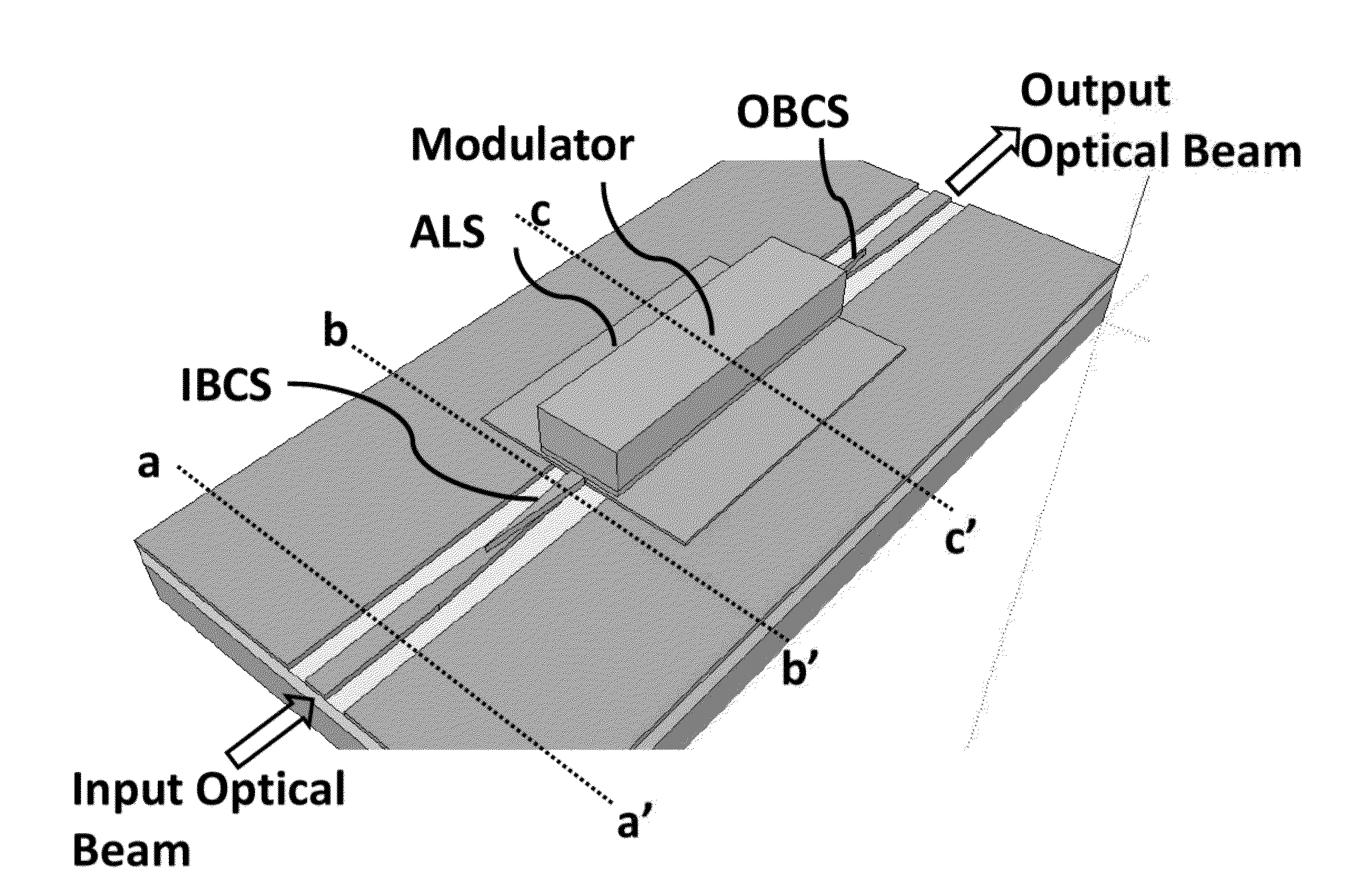
The present invention provides small and efficient intensity or phase modulators with low switching voltage and high modulation bandwidth. These modulators have very low optical loss and can be easily integrated. The invention also includes a waveguiding structure that tapers down to a width smaller than a wavelength, which pushes the mode away from the lower transparent waveguiding structure towards the quantum wells or bulk material, thereby increasing the optical mode energy overlapping with the quantum wells or bulk material. Overall, these technical effects provide modulators with exceptional performance and compactness.

Problems solved by technology

Normally, such thin waveguiding layer can increase the device insertion loss as it is hard to couple light into the layer optically, especially from an optical fiber.

Method used


Image

  • Thin Layer Photonic Integrated Circuit Based Optical Signal Manipulators
  • Thin Layer Photonic Integrated Circuit Based Optical Signal Manipulators
  • Thin Layer Photonic Integrated Circuit Based Optical Signal Manipulators

Examples


Embodiment Construction

Motivations of the Present Invention

[0127]There are various needs for ultra-low-RF-power ultra-wide-RF-bandwidth low-optical-loss high-optical-power modulators for various applications. Certain exemplary modulators employing exemplary embodiments of the present invention are capable of either Ultra Low Voltage, Ultra-High Modulation Bandwidth, Low Optical Loss, or High Optical Power, or a plurality of the above. In addition, they are generally ultra-compact, can be integrated with semiconductor laser, and can be made based on mass-producible silicon-photonic platform with EPIC (electronic-photonic integrated circuit) capability enabling future expansions to integrate with RF circuits or other photonic devices on chip.

Needs for Compact Wide-Bandwidth Low-Power Low-Loss Modulators

[0128]New applications in communications and sensing require transmission of high-frequency electronic signals. Transmission of ultra-fast digital data over optical fiber system is also important for next gen...


PUM


Abstract

Integrated optical intensity or phase modulators capable of very low modulation voltage, broad modulation bandwidth, low optical power loss for device insertion, and very small device size are of interest. Such modulators can be of electro-optic or electro-absorption type made of an appropriate electro-optic or electro-absorption material in particular or referred to as an active material in general. An efficient optical waveguide structure for achieving high overlapping between the optical beam mode and the active electro-active region leads to reduced modulation voltage. In an embodiment, ultra-low modulation voltage, high-frequency response, and very compact device size are enabled by a semiconductor modulator device structure, together with an active semiconductor material that is an electro-optic or electro-absorption material, that are appropriately doped with carriers to substantially lower the modulator voltage and still maintain the high frequency response. In another embodiment, an efficient optical coupling structure further enables low optical loss. Various embodiments combined enable the modulator to reach lower voltage, higher frequency, low optical loss, and more compact size than previously possible in the prior arts.

Description

CROSS-REFERENCES TO RELATED APPLICATIONS[0001]The present application claims priority to U.S. Provisional Application No. 61 / 832,940, filed Jun. 9, 2013; U.S. Provisional Application No. 61 / 833,488, filed Jun. 11, 2013; and U.S. Provisional Application No. 61 / 913,945, filed Dec. 10, 2013, the contents of which are incorporated herein by reference in their entireties.BACKGROUND[0002]The present invention relates to semiconductor photonic, discrete optic, integrated optic, and opto-electronic devices. In particular, the present invention relates to integrated optical modulators capable of modulation of the light beam intensity or phase by an electrical signal. Such modulators are required for converting electrical signals into optical signals so that the light beam can be used to transmit information over an optical communication system. The light source in an optical communication system is typically a semiconductor laser and the transmission of light is typically via an optical fibe...

Claims


Application Information

Patent Timeline
IPC IPC(8): G02F1/025G02F1/017G02B6/122G02B6/12G02F1/19G02F1/17
CPCG02F1/025G02F1/19G02F1/17G02B6/1225G02F2001/0157G02B6/12002G02F1/01708G02B2006/12142G02F2001/0154G02B6/1228G02F1/015G02F1/0152G02F1/0157G02F1/0154
Inventor HUANG, YINGYAN
Owner HO SENG TIONG
Learn More