Optoelectronic Device

a technology of optoelectronic devices and optical emission intensity, which is applied in the direction of semiconductor devices, diodes, electrical apparatus, etc., can solve the problems of low poor optical emission intensity of visible wavelength leds to date, and affecting the concentration of electrons or hole carriers. , to achieve the effect of improving the activation energy of an intentionally doped region and improving the concentration of electrons or hole carriers

Active Publication Date: 2016-05-26
SILANNA UV TECH PTE LTD
View PDF7 Cites 43 Cited by
  • Summary
  • Abstract
  • Description
  • Claims
  • Application Information

AI Technical Summary

Benefits of technology

[0099]Suitably, at least a portion of the at least one of the one or more superlattices includes uniaxial strain or a biaxial

Problems solved by technology

Although it has been possible to produce optoelectronic devices, such as light emitting diodes (LEDs), that emit light in the deep ultra-violet (UV) wavelengths (λ≦280 nm) using group III metal nitride semiconductor materials, such as aluminium gallium nitride (AlGaN), the optical emission intensity from such LEDs to date has been relatively poor compared to visible wavelength LEDs.
This is partly due to an inherent limitation in the AlGaN semiconductor material electronic band structure.
It is found that the emission of deep ultraviolet light from crystalline AlGaN films in a direction substantially parallel to the layer formation growth axis is not favourable in traditional LED structures.
Such high aluminium content compositions are particularly affected by the aforementioned limitation.
It has been widely believed that a poor deep ultraviolet emission intensity in such LEDs is due to an inferior crystalline structural quality of deposited group III metal nitride materials which leads to poor electrical behaviour of the LEDs.
However, even if AlN substrates are available, the deep ultraviolet LED formed using high aluminium content AlGaN materials is still unable to emit light efficiently in a vertical direction (i.e., parallel light emission perpendicular to the plane of the layer).
Yet a further problem exists in the prior art for operation of LEDs based on group III metal nitrides.
Furthermore, each and every different AlGaN composition possesses a slightly different crystal lattice parameter, and therefore each dissimilar AlGaN layer readily forms crystal misfit dislocations at the interface boundary which propagate into the interior of the layer if not correctly managed.
If the dissimilar AlGaN layers are formed to minimize the crystal misfit dislocations, then

Method used


Image

  • Optoelectronic Device
  • Optoelectronic Device
  • Optoelectronic Device

Examples


second embodiment

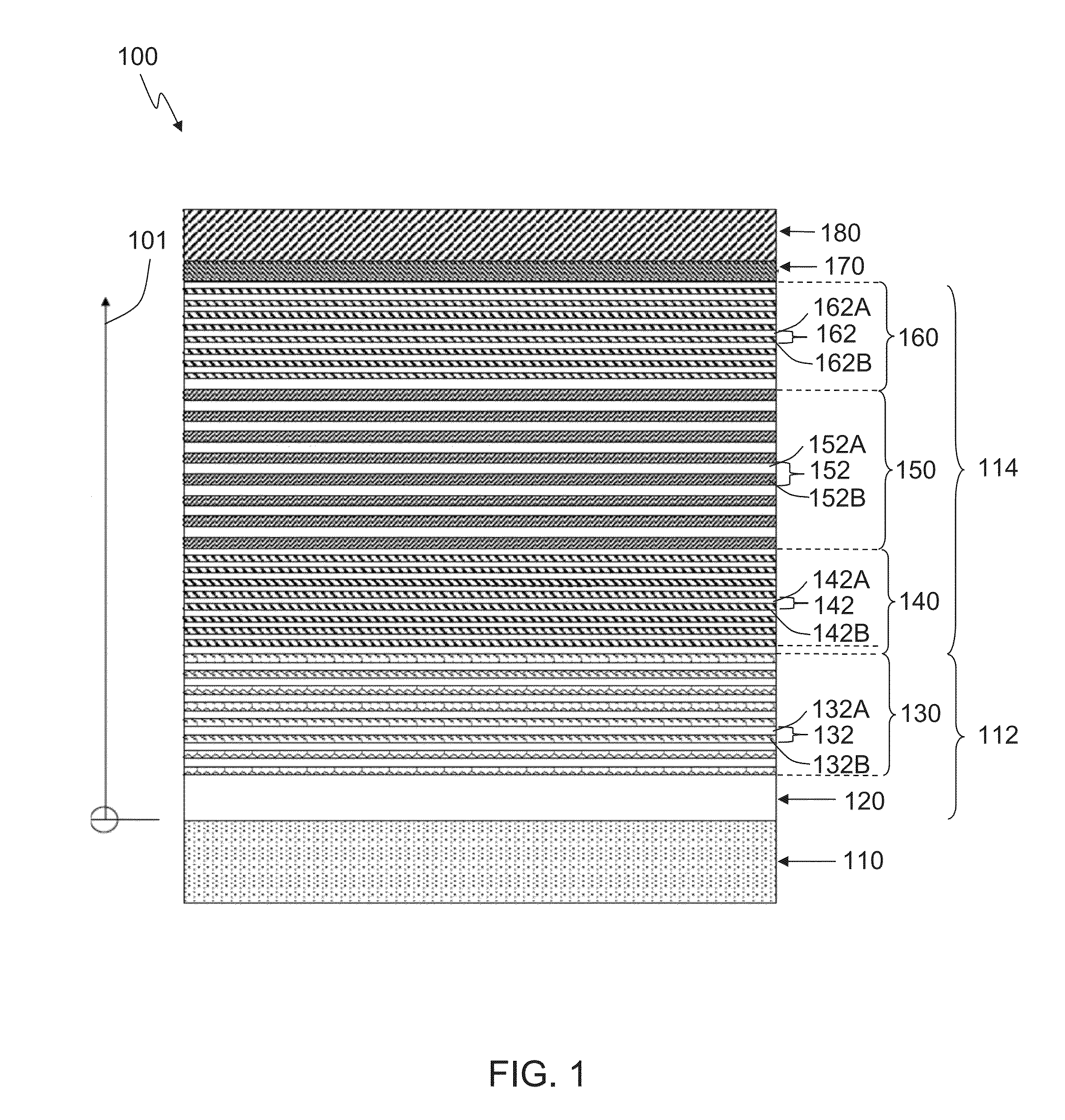
[0218]FIG. 2 is a diagram showing a sectional view of a stack 200 for an optoelectronic device according to the present invention. The stack 200 is similar to the stack 100 of FIG. 1 except that the buffer region 112 does not comprise the one or more superlattices 130.

third embodiment

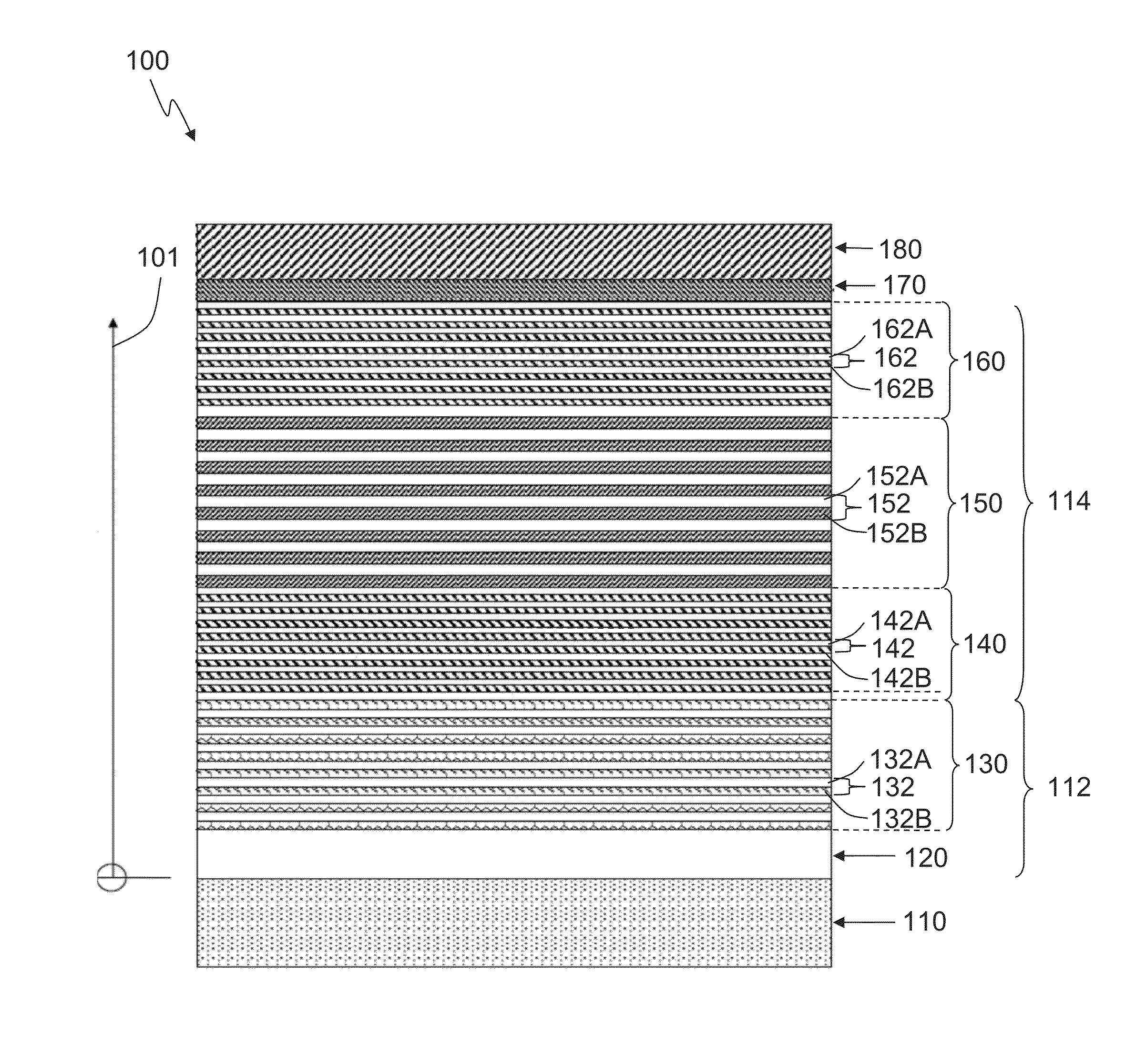
[0219]FIG. 3 is a diagram showing a sectional view of an optoelectronic device 300 according to the present invention. Similar to the stacks 100 and 200 of FIGS. 1 and 2, the optoelectronic device 300 comprises a substrate 110 on which a buffer layer 120 and a semiconductor structure 114 are formed. The semiconductor structure 114 comprises, in growth order, an n-type active region 140, an i-type active region 150 and a p-type active region 160. A p-type contact layer 170 is formed on the p-type active region 160 and a first contact layer 180 is formed on the p-type contact layer 170.

[0220]In the embodiment shown in FIG. 3, the i-type active region 150, the p-type active region 160, p-type contact layer 170 and the first contact layer 180 form a mesa on the n-type active region 140. The mesa shown in FIG. 3 has straight sidewalls. However, in alternative embodiments, the mesa can have angled side walls. The device 300 further comprises a second contact layer 382 formed on the n-type...

fourth embodiment

[0222]FIG. 4 is a diagram showing a sectional view of an optoelectronic device 400 according to the present invention. The optoelectronic device 400 is similar to the optoelectronic device300 of FIG. 3. However, the optoelectronic device comprises a first lateral contact 486 and a second lateral contact 484.

[0223]The first lateral contact 486 extends partially into the p-type active region 160 from the first contact layer 180. In preferred embodiments, the first lateral contact 486 is an annular shaped protrusion extending from the first contact layer 180 into in the p-type active region 160 and (where applicable) the p-type contact layer 170. In some embodiments, the first lateral contact 486 is made from the same material as the first contact layer 180.

[0224]The second lateral contact 484 extends partially into the n-type active region 140 from the second contact layer 482 formed on a surface of the n-type active region 140. In preferred embodiments, the second lateral contact 484...


PUM


Abstract

An optoelectronic device comprising a semiconductor structure includes a p-type active region and an n-type active region. The semiconductor structure is comprised solely of one or more superlattices, where each superlattice is comprised of a plurality of unit cells. Each unit cell comprises at least two distinct substantially single crystal layers.

Description

CROSS-REFERENCE TO RELATED APPLICATION[0001]This application is a continuation of International Patent Application number PCT / IB2014 / 052480, filed Apr. 6, 2015, which claims priority to Australian Provisional Patent Application number 2014902007, filed May 27, 2014 and entitled “An Optoelectronic Device”, both of which are incorporated herein by reference in their entirety.FIELD OF THE INVENTION[0002]This invention relates generally to optoelectronic devices. In particular, the invention relates to optoelectronic devices that emit light at ultra-violet wavelengths. However, the invention is not limited to ultraviolet wavelengths.BACKGROUND OF THE INVENTION[0003]Although it has been possible to produce optoelectronic devices, such as light emitting diodes (LEDs), that emit light in the deep ultra-violet (UV) wavelengths (λ≦280 nm) using group III metal nitride semiconductor materials, such as aluminium gallium nitride (AlGaN), the optical emission intensity from such LEDs to date has...

Claims


Application Information

Patent Timeline
IPC IPC(8): H01L33/06H01L33/32H01L33/46H01L33/18H01L33/10
CPCH01L33/06H01L33/18H01L33/325H01L33/46H01L33/105H01L33/04H01L33/0045H01L33/007H01L33/08H01L33/32H01L33/382H01L33/0008H01L2924/12041
Inventor ATANACKOVIC, PETAR
Owner SILANNA UV TECH PTE LTD
Why Eureka
Try Eureka