Method for Forming an Electrical Contact

a technology of electrical contact and junction performance, applied in the direction of electrical apparatus, semiconductor device details, semiconductor/solid-state device devices, etc., can solve the problems of degrading junction performance, reducing contact resistance, and ignoring the challenge of reducing contact resistance, so as to simplify the electrical contact formation

Active Publication Date: 2016-06-09
INTERUNIVERSITAIR MICRO ELECTRONICS CENT (IMEC VZW)
View PDF11 Cites 12 Cited by
  • Summary
  • Abstract
  • Description
  • Claims
  • Application Information

AI Technical Summary

Benefits of technology

[0054]Advantageously, the method described may be particularly suited for producing NiGe or NiSi electrical contacts in this integrated circuit that may comprise multiple n-MOS and p-MOS field effect transistors. The method described simplifies the electrical contact formation. NiGe or NiSi electrical contacts may be formed simultaneously on p-MOS and n-MOS field effect transistors, respectively, thanks to the advantage that NiGe or NiSi formation, by the method described, is independent of the underlying layer.
[0055]If, this p-MOS and this n-MOS field effect transistor or plurality of n-MOS and p-MOS field effect transistors is/are desired to have different electrical contacts, for example NiGe on p-MOS field effect transistor and NiSi on n-MOS field effect transistor or NiGe on n-MOS field effect transistor and NiSi on p-MOS field effect transistor, then after Ni deposition, a protective laye

Problems solved by technology

This approach faces several challenges as CMOS scaling continues.
Firstly, the consumption of Ge during the germanidation reaction jeopardizes the geometry of the source and/or drain regions thus degrading the junction performances due to the dopants being pushed down to the Ge layers.
Furthermore, the Ge material consumption results in formed germanide extending deeper into the Ge than the junction thereby forming short-circuit to underlying substrate.
However, such

Method used


Image

  • Method for Forming an Electrical Contact
  • Method for Forming an Electrical Contact
  • Method for Forming an Electrical Contact

Examples


Embodiment Construction

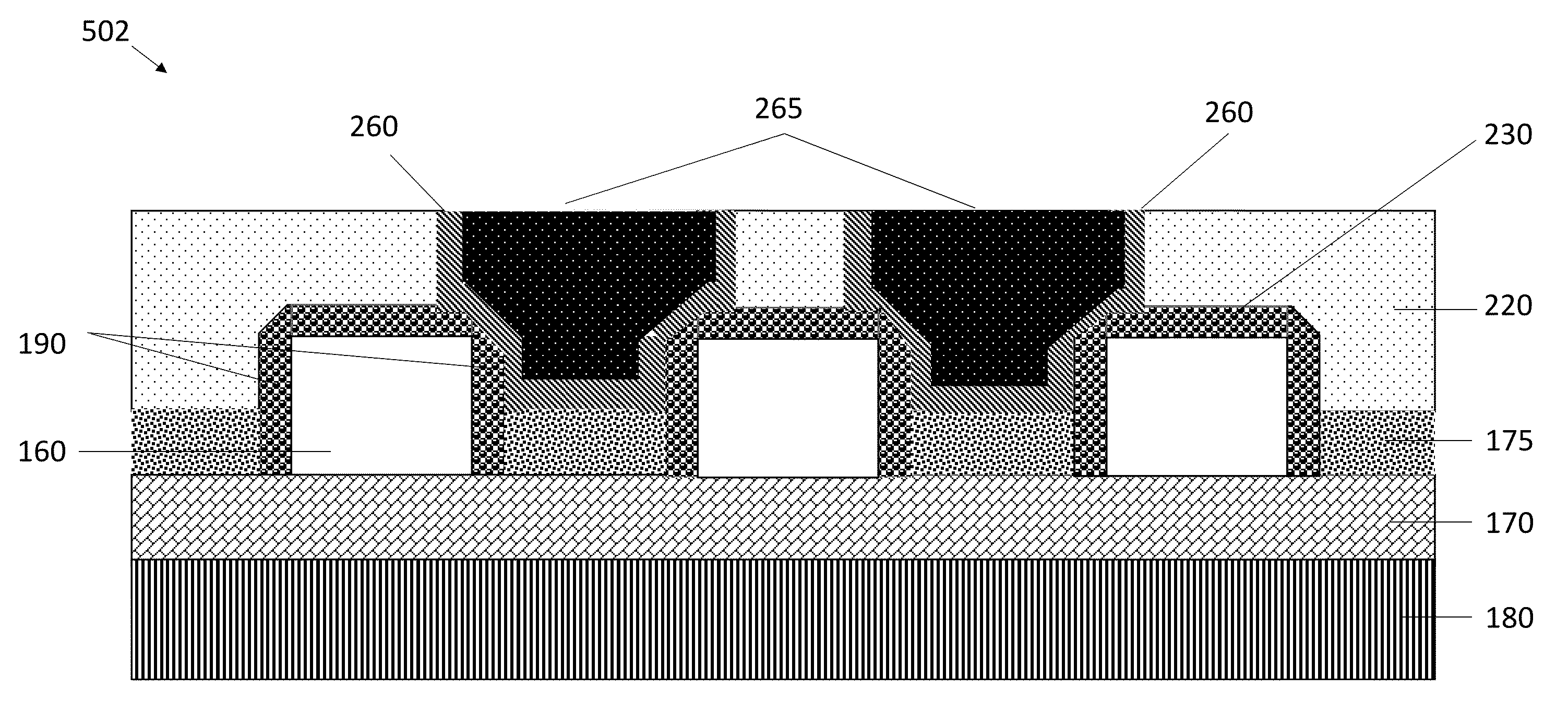
[0072]The present invention will be described with respect to particular embodiments and with reference to certain drawings but the invention is not limited thereto but only by the claims. The drawings described are only schematic and are non-limiting. In the drawings, the size of some of the elements may be exaggerated and not drawn on scale for illustrative purposes. The dimensions and the relative dimensions do not correspond to actual reductions to practice of the invention.

[0073]Reference throughout this specification to “one embodiment” or “an embodiment” means that a particular feature, structure or characteristic described in connection with the embodiment is included in at least one embodiment of the present invention. Thus, appearances of the phrases “in one embodiment” or “in an embodiment” in various places throughout this specification are not necessarily all referring to the same embodiment, but may. Furthermore, the particular features, structures or characteristics m...


PUM


Abstract

A method for forming an electrical contact to a semiconductor structure is provided. The method includes providing a semiconductor structure, providing a metal on an area of said semiconductor structure, wherein said area exposes a semiconductor material and is at least a part of a contact region, converting said metal to a Si-comprising or a Ge-comprising alloy, thereby forming said electrical contact on said area, wherein said converting is done by performing a vapor-solid reaction, whereby said semiconductor structure including said metal is subjected to a silicon-comprising precursor gas or a germanium-comprising precursor gas.

Description

CROSS-REFERENCE[0001]This application claims priority from European Patent Application No. EP 14196804.0, filed Dec. 8, 2014, which is incorporated by references in its entirety.TECHNICAL FIELD OF THE INVENTION[0002]The present invention is related to the field of contact formation. More specifically, it is related to a method for forming an electrical contact to a semiconductor structure, whereby a metal-semiconductor alloy is used. The present invention also relates to semiconductor devices comprising electrical contacts obtained thereby.BACKGROUND OF THE INVENTION[0003]The effort to keep up with CMOS scaling, which relates to reducing the size of transistors in pursuit of Moore's Law, has led semiconductor industry in search for new transistor designs and use of alternative materials. In terms of design improvement, multi gate field effect transistors (MUGFET), such as FinFETs and Tri-gate FETs, are one of the strategies implemented. A MUGFET is a term used to describe a metal ox...

Claims


Application Information

Patent Timeline
IPC IPC(8): H01L23/535H01L23/532H01L29/08H01L21/768
CPCH01L23/535H01L21/76805H01L29/0847H01L21/76895H01L23/53209H01L21/76886H01L21/28518H01L21/76843H01L21/76856H01L2924/0002H01L21/02532H01L29/41791H01L21/0262H01L21/02653H01L21/02425H01L2924/00H01L21/244H01L21/24
Inventor PETER, ANTONY PREMKUMARSCHAEKERS, MARC
Owner INTERUNIVERSITAIR MICRO ELECTRONICS CENT (IMEC VZW)
Why Eureka
Try Eureka