Isotropic atomic layer etch for silicon oxides using no activation

a silicon oxide and atomic layer technology, applied in the direction of electrical equipment, basic electric elements, electric discharge tubes, etc., can solve the problems of high undesired native oxide and other oxides, limited control methods of one or several atomic layers, and difficulty in further processing steps

Active Publication Date: 2016-07-07
LAM RES CORP
View PDF1 Cites 286 Cited by
  • Summary
  • Abstract
  • Description
  • Claims
  • Application Information

AI Technical Summary

Problems solved by technology

While atomic layer deposition (ALD) and atomic-scale epitaxial growth techniques have been developed, the methods for controlled removal of one or several atomic layers are still limited.
Silicon oxide also is inadvertently formed on layers of silicon when a partially fabricated wafer is exposed to air.
Native oxide film together with oxide residue produced during etching and/or ashing frequently presents a problem for further processing steps.
When formed in the bottom of a silicon landed via or conta...

Method used


Image

  • Isotropic atomic layer etch for silicon oxides using no activation
  • Isotropic atomic layer etch for silicon oxides using no activation
  • Isotropic atomic layer etch for silicon oxides using no activation

Examples


example

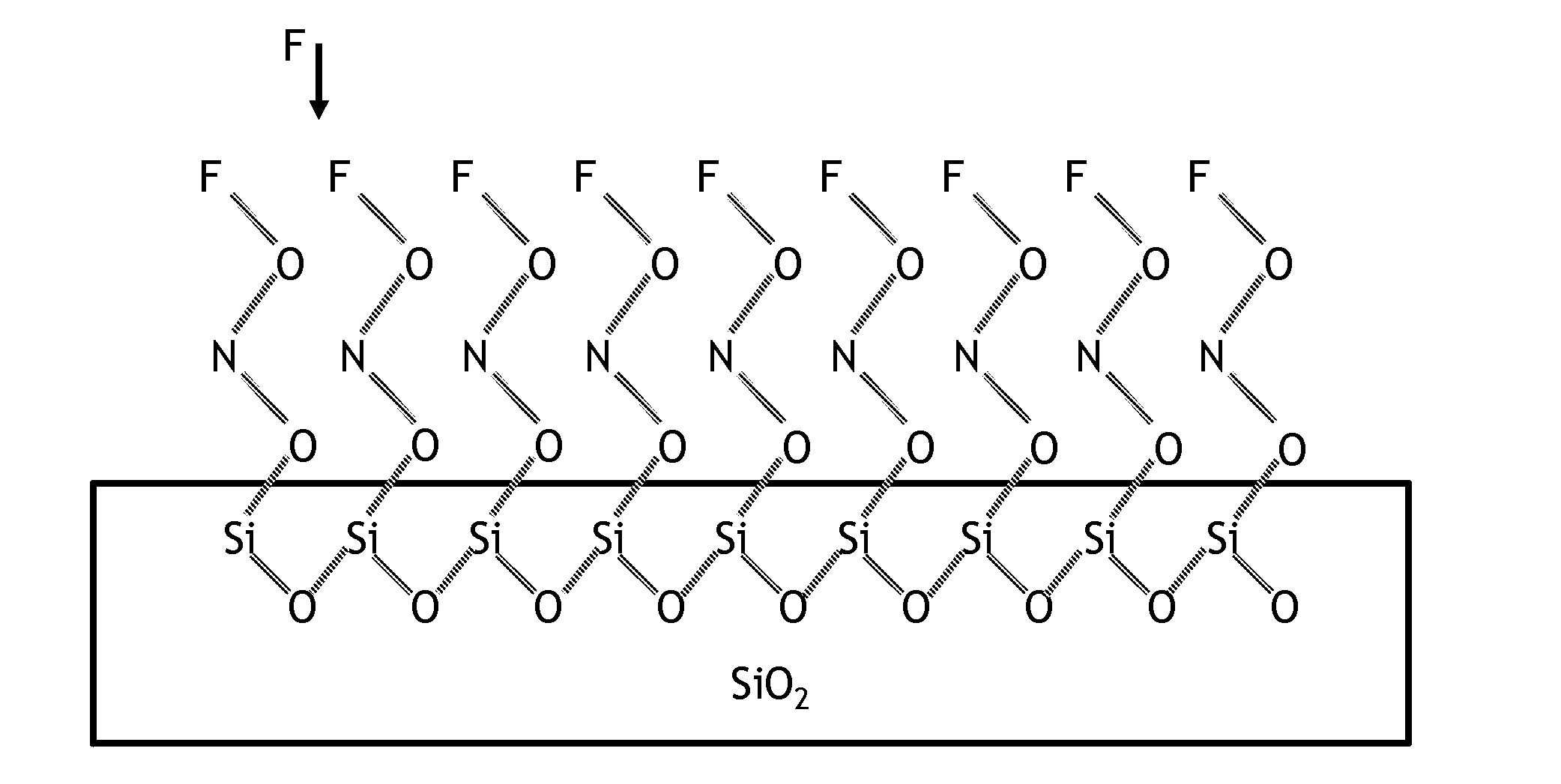
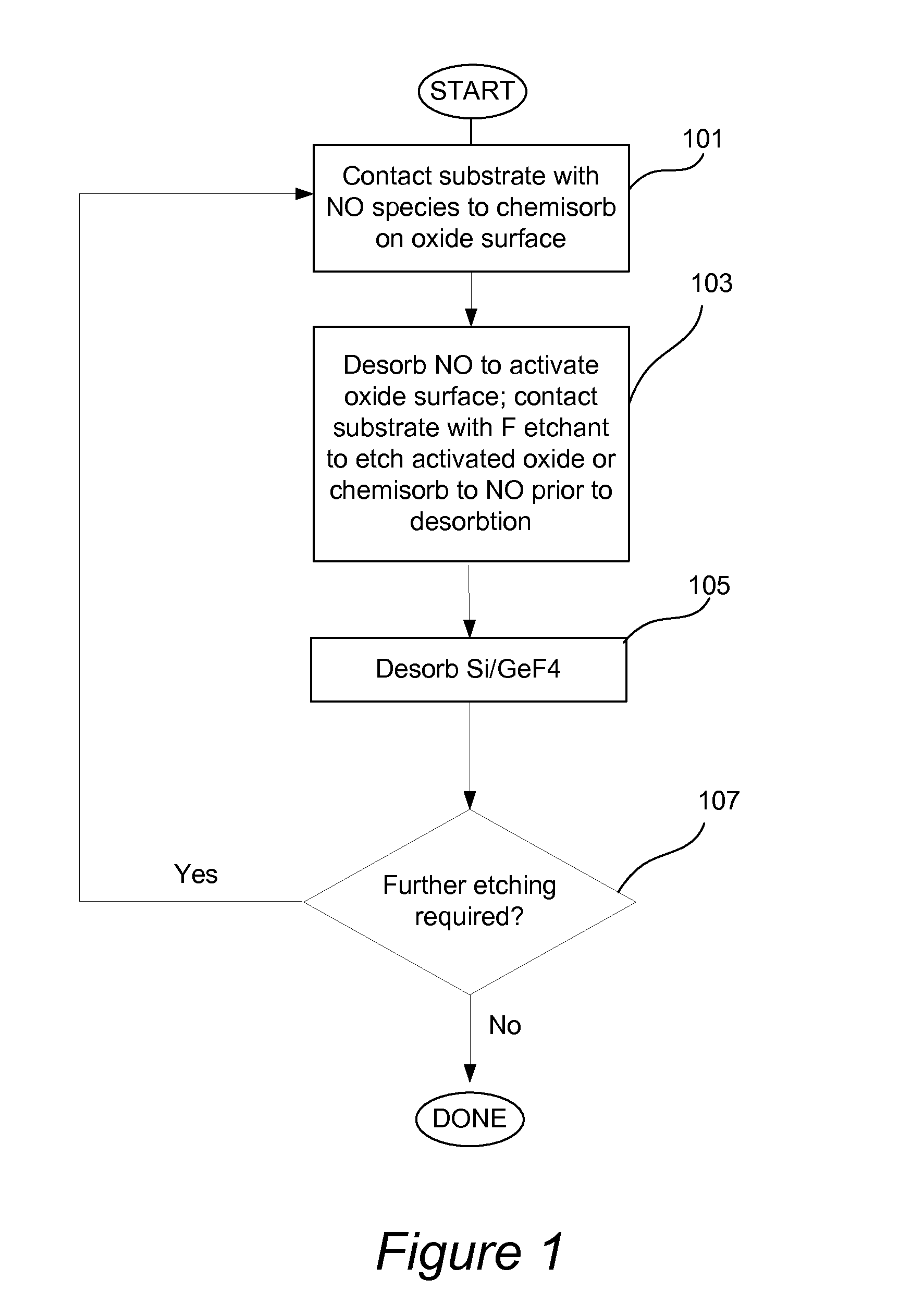
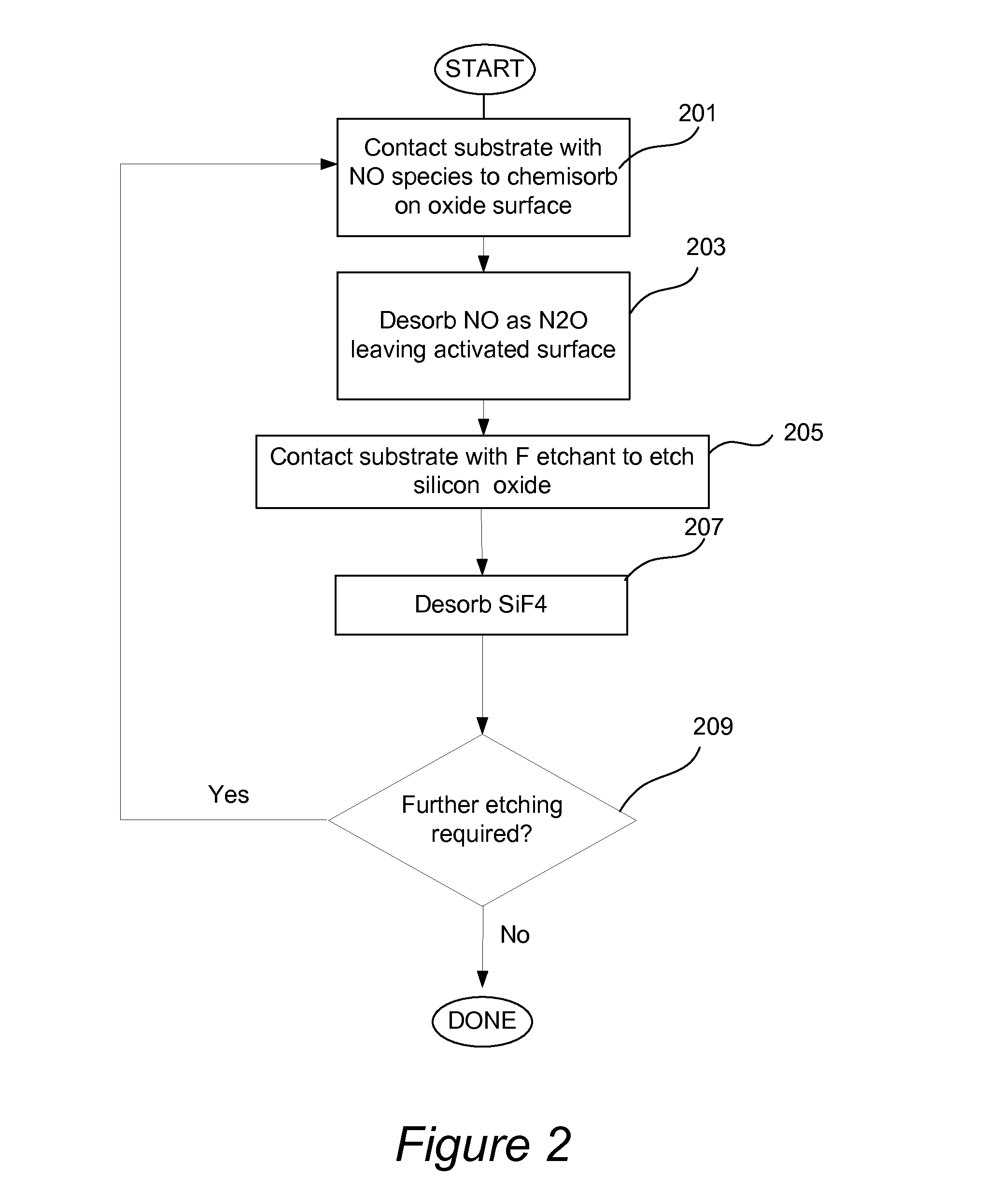
[0052]In order to more fully illustrate features of a specific embodiment, the following non-limiting example of an etch process in accordance with FIGS. 4 and 5 is provided. An example of an etch process is to 1) load a substrate containing an oxide into a vacuum housing; 2) optionally pre-treat the sample to remove surface oxides or silanol bonds; 3) strike a plasma of NO gas (or a gas mixture of about 50% O2+50% N2O by volume) at 1.0-3.0 Torr to passivate the oxide surface; 4) add a fluorine containing gas to the plasma such as CF4 (about 5-7% by volume); 5) turn off the plasma and fluorine source and let the NO desorb and initiate etching; 6) optionally purge the vacuum chamber with an inter gas such as nitrogen or argon; 7) repeat steps 3-6 as needed to etch target film thickness.

[0053]Apparatus

[0054]The methods described herein can be practiced in a variety of apparatuses that are equipped with delivery lines and control mechanisms configured for sequential delivery of gaseous...


PUM

PropertyMeasurementUnit
Temperatureaaaaaaaaaa
Angleaaaaaaaaaa

Abstract

Methods for controlled isotropic etching of layers of silicon oxide and germanium oxide with atomic scale fidelity are provided. The methods make use of NO activation of an oxide surface. Once activated, a fluorine-containing gas or vapor etches the activated surface. Etching is self-limiting as once the activated surface is removed, etching stops since the fluorine species does not spontaneously react with the un-activated oxide surface. These methods may be used in interconnect pre-clean applications, gate dielectric processing, manufacturing of memory devices, or any other applications where accurate removal of one or multiple atomic layers of material is desired.

Description

FIELD OF THE INVENTION[0001]The present invention pertains to methods of removing layers of material on a substrate. The methods are particularly useful for accurate isotropic removal of silicon dioxide and germanium dioxide with atomic scale fidelity on a semiconductor substrate.BACKGROUND OF THE INVENTION[0002]Fabrication of integrated circuit (IC) devices at a modern level of miniaturization demands techniques that can operate at an atomic scale. Certain components of IC devices now have dimensions of tens of Angströms, corresponding to only a few atomic layers of material. For example, gate dielectric in modern IC transistors can have a thickness of only 12 Å, corresponding to only four atomic layers of silicon dioxide. It is often desirable to fine-tune the electronic properties of these components by altering their dimensions, which would involve deposition or removal of only a few atomic layers of material. While atomic layer deposition (ALD) and atomic-scale epitaxial growth...

Claims


Application Information

Patent Timeline
IPC IPC(8): H01L21/02H01L21/311
CPCH01L21/02252H01L21/31144H01L21/31116H01J37/32449H01L21/31122H01L21/02057H01J37/32009H01J37/32715H01J2237/334H01L21/0274H01L21/67069
Inventor BERRY, III, IVAN L.PARK, PILYEONYAQOOB, FAISAL
Owner LAM RES CORP
Why Eureka
Try Eureka