

Methods of growing heteroepitaxial single crystal or large grained semiconductor films and devices thereon
- Summary
- Abstract
- Description
- Claims
- Application Information
AI Technical Summary
Benefits of technology
Problems solved by technology
Method used
Image

Examples
example of invention
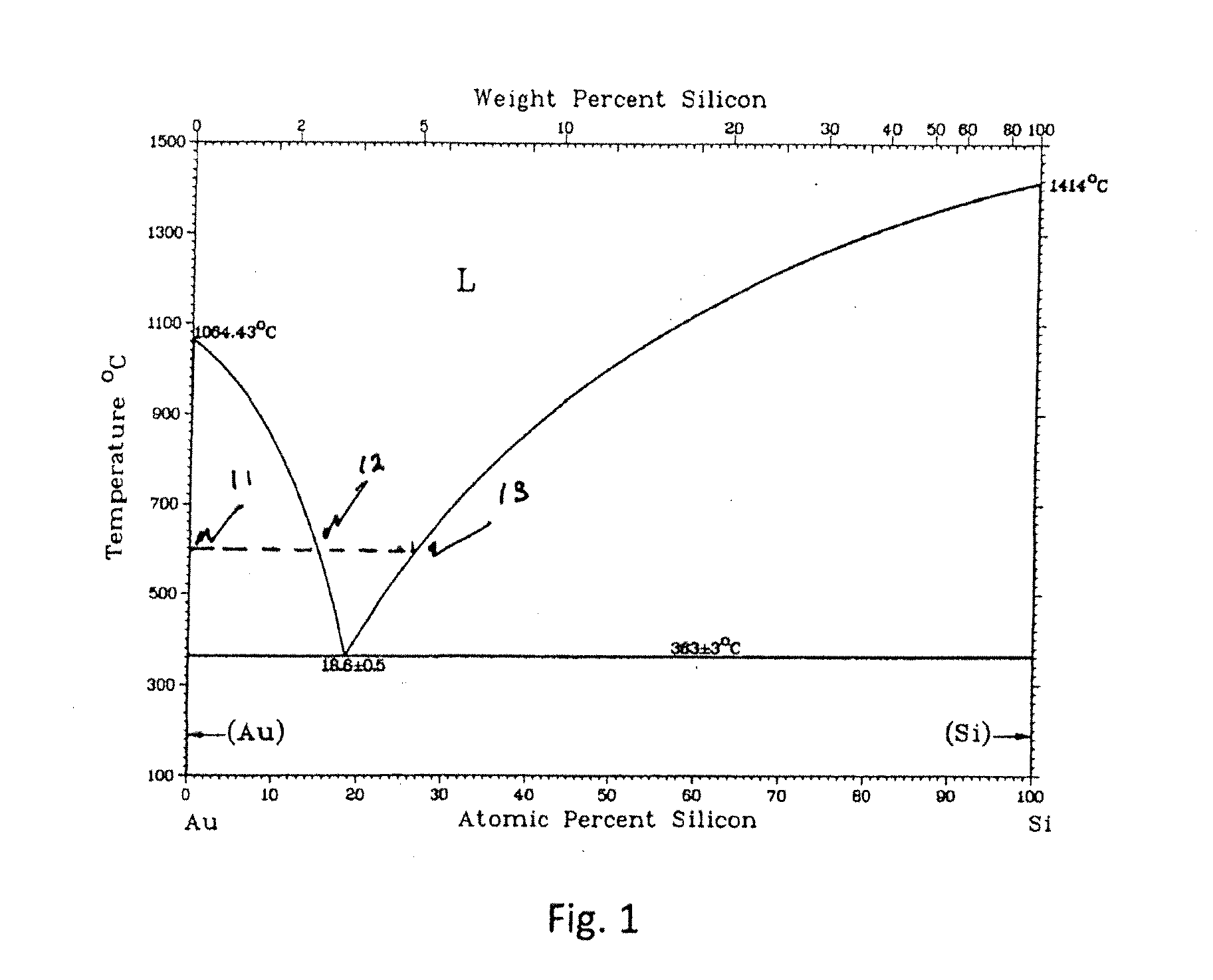
[0048]A good high vacuum system with two electron beam guns, is used to deposit tin and silicon independently. A glass substrate coated with textured MgO is held at temperatures between 575 and 600° C. These are nominal temperatures. It is understood to one skilled in the art that lower or higher temperatures can also be used depending upon the softening temperature 7802236.1 of the glass substrate or the reaction kinetics of either tin or silicon with the MgO layers when used a substrates. A thin tin film of approximately 10 nm thickness is deposited first. This is followed by a silicon film deposited at a rate of 2 nm per minute on top of the tin film. The silicon film nucleates heterogeneously on the MgO surface to form the desired thin film. The film can now be cooled to room temperature, where the film now comprises of two phases: tin and a relatively large grained and highly textured film of silicon on MgO. The tin diffuses to the surface of the silicon film, driven by its low...
PUM
| Property | Measurement | Unit |
|---|---|---|
| Transparency | aaaaa | aaaaa |
| Semiconductor properties | aaaaa | aaaaa |
Abstract
Description
Claims
Application Information