Switch device and storage unit

Active Publication Date: 2016-11-17
SONY SEMICON SOLUTIONS CORP
View PDF4 Cites 35 Cited by
  • Summary
  • Abstract
  • Description
  • Claims
  • Application Information

AI Technical Summary

Benefits of technology

[0074]It is to be noted that when the switch layer 30 is too thin, depending on leakage characteristics during non-selection of the materials of the switch layer 30, it is difficult to reduce the leakage current, and the OTS phenomenon is less likely to be caused. Moreover, when the switch layer 30 is too thick, an issue arises in a miniaturization process. Reducing a device size makes it possible to increase a switching threshold voltage, thereby reducing the leakage current. In a miniaturized switch device (a fine device), there is a tendency that a too thick thickness causes an increase in aspect ratio (a size in a plane direction: a size in a vertical direction (a stacking direction)), thereby causing a difficulty in microfabrication. Accordingly, the thickness of the switch layer 30 may be preferably within a range of 5 nm to 100 nm both inclusive.
[0075]The upper electrode 20 may use a known semiconductor wiring material as with the lower electrode 10. A stable material that does not react with the switch layer 30 even after post annealing may be preferable.
[0076]As described above, the switch device 1 according to this embodiment reduces resistance by applying a voltage equal to or higher than a certain voltage without phase change between an amorphous phase and a crystalline phase, and returns to a high-resistance state by reducing the applied voltage to a voltage lower than the certain voltage. The certain voltage is referred to as a switching threshold voltage. In other words, in the switch device 1, a phase change is not caused in the switch layer 30 by application of a voltage pulse or a current pulse from an unillustrated power supply circuit (a pulse application section) through the lower electrode 10 and the upper electrode 20. Moreover, the switch device 1 does not perform a memory operation such as maintaining a transmission path formed by ion movement by voltage application even after erasing the applied voltage. Further, the switch device 1 according to this embodiment is used as a selection device that selectively operates a ce

Problems solved by technology

Therefore, in a case in which such a memory device is used to achieve a high-capacity memory, the switching threshold voltage of the above-described OTS device is not sufficiently high.
Although increasing a thic

Method used


Image

  • Switch device and storage unit
  • Switch device and storage unit
  • Switch device and storage unit

Examples


first embodiment

1. First Embodiment

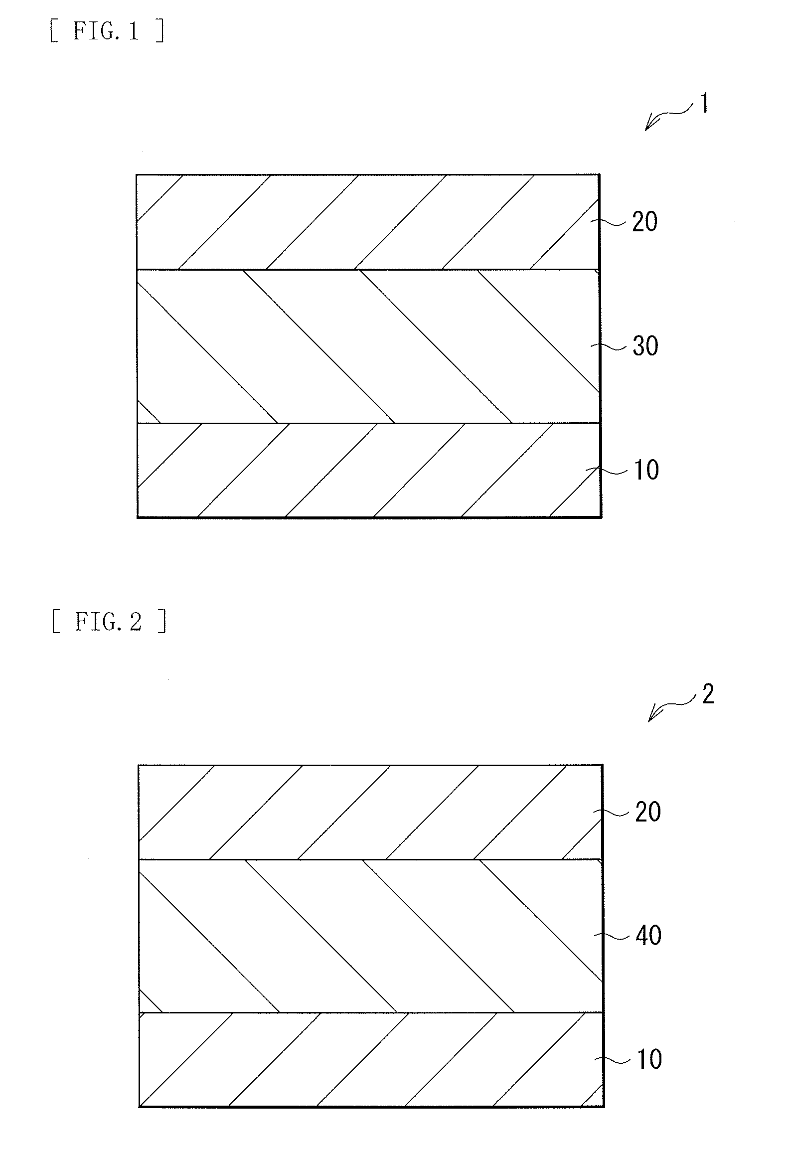
[0064]FIG. 1 illustrates a cross-sectional configuration of a switch device 1 according to a first embodiment of the disclosure. The switch device 1 is adapted to selectively operate a certain storage device (a storage device 6Y; refer to FIG. 7) of a plurality of storage devices arranged in a memory cell array with, for example, a so-called cross-point array configuration illustrated in FIG. 7. The switch device 1 (a switch device 6X; refer to FIG. 7) is coupled in series to the storage device 6Y (more specifically, a storage layer 70), and includes a lower electrode 10 (a first electrode), a switch layer 30, and an upper electrode 20 (a second electrode) in this order. It is to be noted that the switch device 1 is adapted to change its resistance state upon application of a predetermined voltage without phase change (between an amorphous state and a crystalline phase).

[0065]The lower electrode 10 may be made of a wiring material used in a semiconductor process. ...

second embodiment

2. Second Embodiment

[0087]FIG. 2 illustrates a cross-sectional configuration of a switch device 2 according to the second embodiment of the disclosure. As with the above-described switch device 1, the switch device 2 is adapted to selectively operate a certain storage device of a plurality of storage devices arranged in a memory cell array with a so-called cross-point array configuration. As with the foregoing first embodiment, the switch device 2 includes the lower electrode 10, a switch layer 40, and the upper electrode 20 in this order.

[0088]The switch layer 40 in this embodiment includes a Group 16 element of the periodic table, more specifically, a chalcogen element such as S, Se, and Te, and further includes an alkaline-earth metal such as Mg, Ca, and Sr, a Group 13 element of the periodic table such as Al and Ga, or a rare earth element such as Y and lanthanoids. These elements are included to be bonded to the chalcogen element, thereby forming a chalcogenide such as MgTe, Ca...

third embodiment

3. Third Embodiment

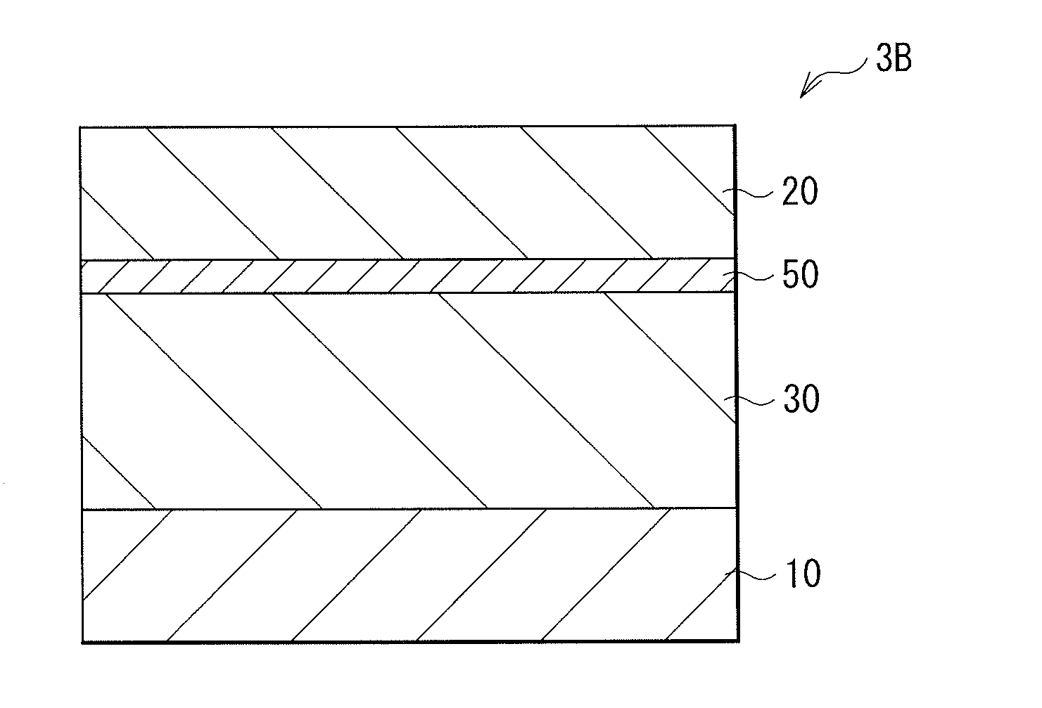
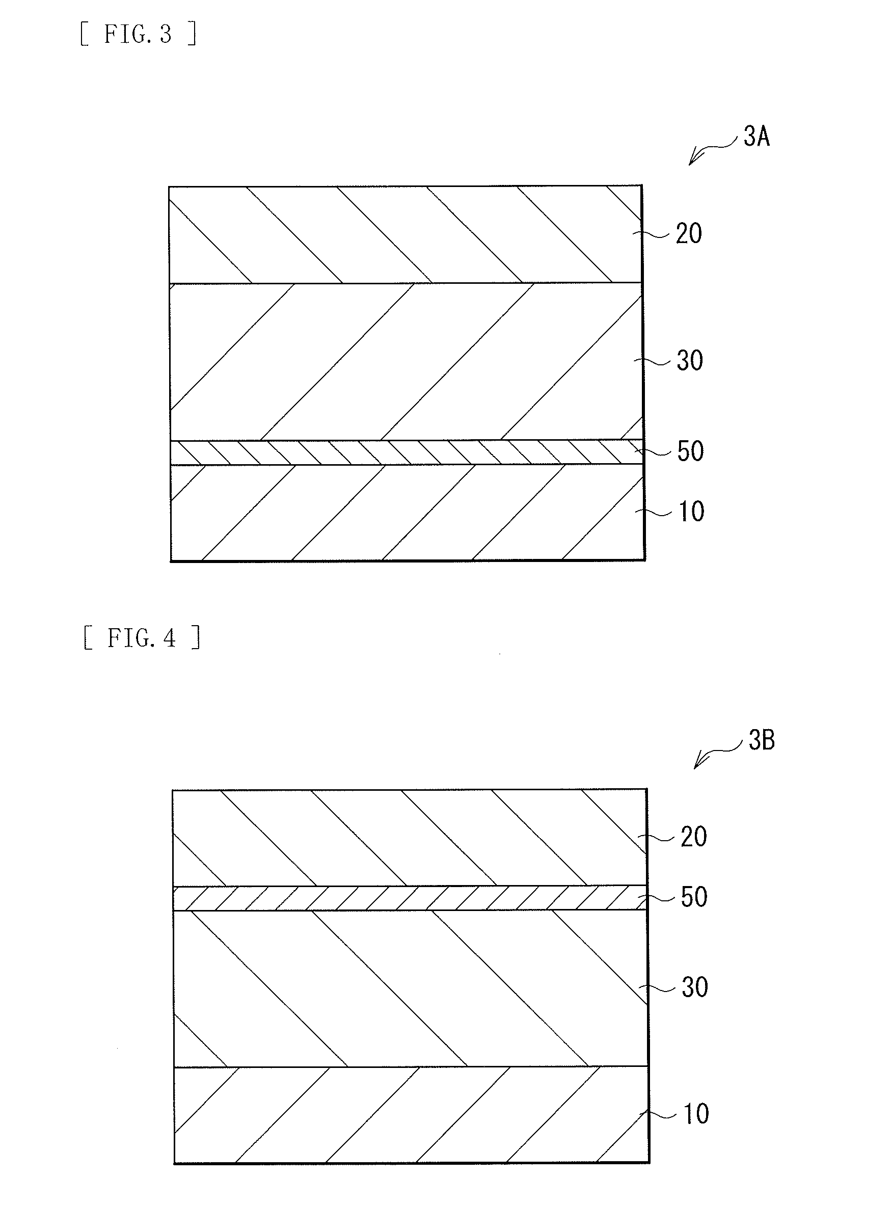
[0094]FIG. 3 illustrates a cross-sectional configuration of a switch device 3A according to the third embodiment of the disclosure. As with the above-described switch device 1, the switch device 3A is adapted to selectively operate a certain storage device of a plurality of storage devices arranged in a memory cell array with a so-called cross-point array configuration. The third embodiment differs from the foregoing first embodiment in that the switch device 3A includes the lower electrode 10, a high-resistance layer 50, the switch layer 30, and the upper electrode 20 in this order, and the high-resistance layer 50 is formed between the lower electrode 10 and the switch layer 30.

[0095]As with the foregoing first embodiment, the switch layer 30 includes a Group 16 element of the periodic table, more specifically, a chalcogen element such as S, Se, and Te, and further includes one or more kinds selected from Si, B, and C that are metalloid light elements, and one o...


PUM


Abstract

A switch device includes: a first electrode; a second electrode disposed to oppose the first electrode; a switch layer provided between the first electrode and the second electrode, and including at least one or more kinds of chalcogen elements and one or more kinds of first elements out of the one or more kinds of chalcogen elements, the one or more kinds of first elements, and a second element including one or both of oxygen (O) and nitrogen (N), the one or more kinds of chalcogen elements being selected from tellurium (Te), selenium (Se), and sulfur (S), and the one or more kinds of first elements being selected from boron (B), carbon (C), and silicon (Si).

Description

TECHNICAL FIELD[0001]The disclosure relates to a switch device and a storage unit that each include a chalcogenide layer between electrodes.BACKGROUND ART[0002]In recent years, an increase in capacity has been demanded in non-volatile memories for data storage. The non-volatile memories for data storage are typified by resistance-change memories such as ReRAMs (Resistance Random Access Memories) and PRAMs (Phase-Change Random Access Memories). However, in a resistance-change memory using an existing access transistor, a floor area per unit cell is increased. Accordingly, for example, as compared with flash memories such as NAND flash memories, it is difficult to achieve an increase in capacity of the resistance-change memory even in a case in which the resistance-change memory is miniaturized with use of same design rules. In contrast, in a case in which the resistance-change memory uses a so-called cross-point array configuration in which memory devices are each provided at corresp...

Claims


Application Information

Patent Timeline
IPC IPC(8): H01L27/24G11C13/00H01L45/00
CPCH01L27/2481H01L45/1233H01L45/142H01L45/143H01L45/144H01L45/1641G11C13/0023H01L45/065G11C13/0069G11C13/004G11C13/0007G11C13/0097H01L45/1608G11C13/0002G11C2013/0073G11C13/0004G11C13/003G11C2213/73G11C2213/76H10B63/24H10B63/80H10N70/20H10N70/8822H10N70/8825H10N70/026H10N70/826H10N70/8828H10N70/882H10N70/041H10B63/84H10N70/021H10N70/235
Inventor OHBA, KAZUHIROSEI, HIROAKI
Owner SONY SEMICON SOLUTIONS CORP
Why Eureka
Try Eureka