Silicon carbide semiconductor device and silicon carbide semiconductor device manufacturing method

a semiconductor device and silicon carbide technology, applied in the direction of semiconductor devices, basic electric elements, electrical equipment, etc., can solve the problems of increasing the conduction loss of the device, increasing the current path in the drift layer, increasing the resistance, etc., to reduce the on resistance and increase the breakdown voltage

Active Publication Date: 2016-11-17
MITSUBISHI ELECTRIC CORP
View PDF24 Cites 250 Cited by
  • Summary
  • Abstract
  • Description
  • Claims
  • Application Information

AI Technical Summary

Benefits of technology

[0017]According to the above-mentioned aspects of the present invention, the doping concentration distribution of the drift layer can be brought close to the doping concentration distribution ideal for reducing the ON resistance, and furthermore, for increasing the breakdown voltage by the achievable technique.
[0018]These and other objects, features, aspects and advantages of the present technology will become more apparent from the following detailed description of the present technology when taken in conjunction with the accompanying drawings.

Problems solved by technology

The silicon carbide power semiconductor device has high breakdown voltage in recent times, and thus the drift layer has a greater thickness, causing a longer current path in the drift layer.
Consequently, drift resistance forms an increasing proportion of ON resistance, which increases a conduction loss of the device.
The greater thickness of the drift layer increases distortion of lattice in the drift layer due to a mismatch in lattice constant between the drift layer and the substrate, and thus a density of crystal defects in the drift layer increases, causing an increase in resistance and a decrease in yields of the device.
For this reason, it is an extremely important challenge to achieve the structure of the device capable of reducing a drift resistance and a density of crystal defects.

Method used


Image

  • Silicon carbide semiconductor device and silicon carbide semiconductor device manufacturing method
  • Silicon carbide semiconductor device and silicon carbide semiconductor device manufacturing method
  • Silicon carbide semiconductor device and silicon carbide semiconductor device manufacturing method

Examples


first embodiment

SBD, Inclined Epitaxy

[0046]

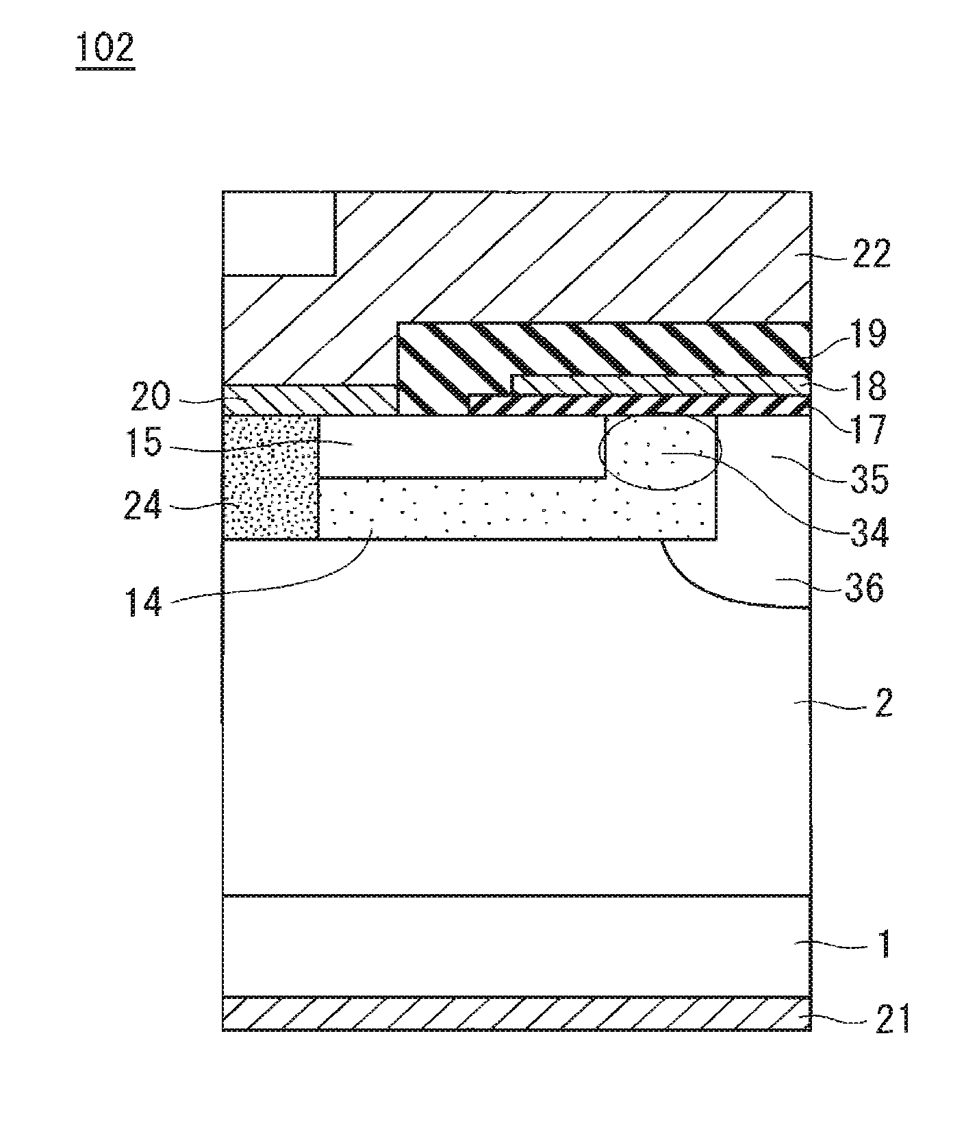
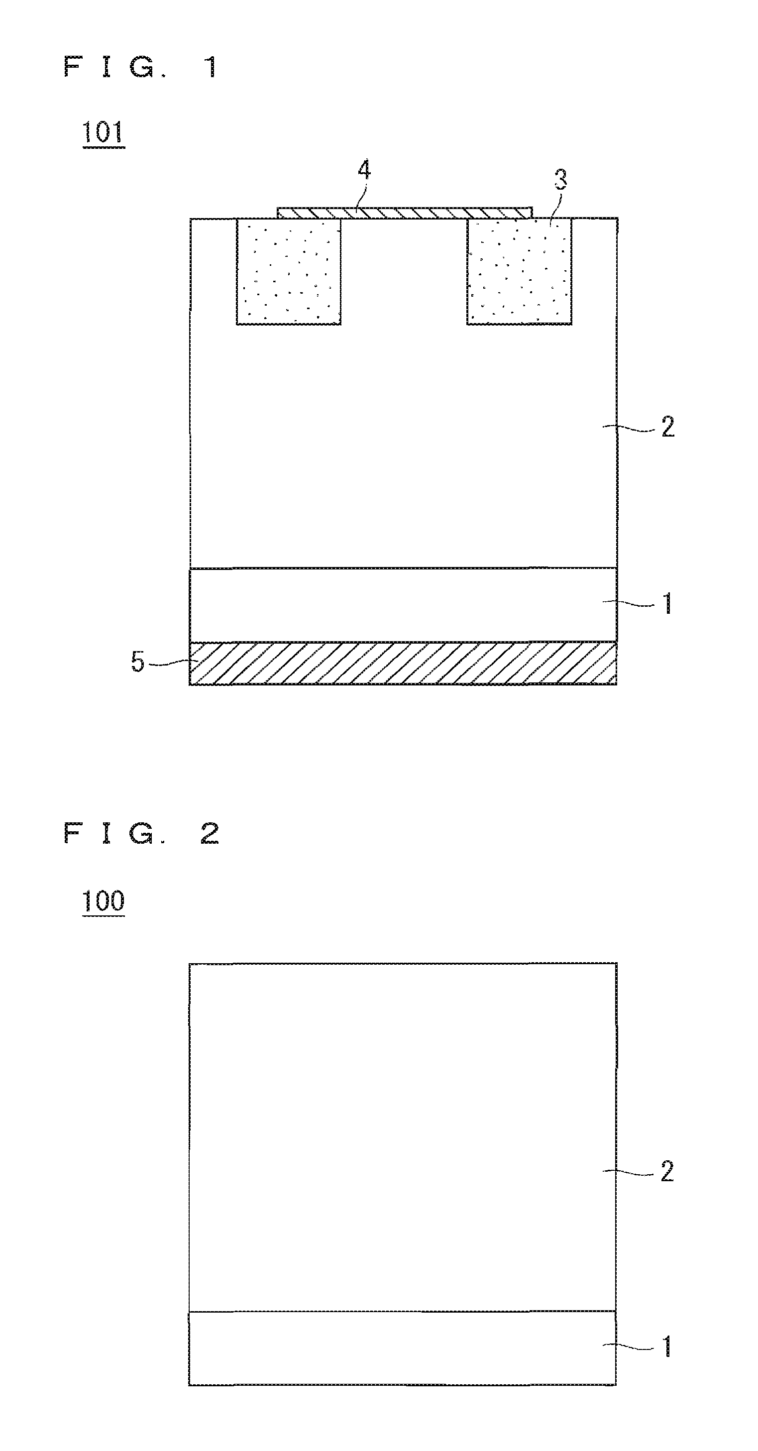
[0047]FIG. 1 is a cross-sectional view showing a configuration of a silicon carbide semiconductor device according to a first embodiment of the present invention. FIG. 2 is a cross-sectional view showing a structure of an epitaxial substrate according to the first embodiment of the present invention.

[0048]As shown in FIG. 2, an epitaxial substrate 100 includes a silicon carbide substrate 1 of the n-type being the first conductivity type that has an off-angle from a 4H—SiC(0001) plane and has a low resistance, and the epitaxial substrate 100 includes a drift layer 2 of the n-type formed on the silicon carbide substrate 1 by epitaxial growth.

[0049]It is sufficient as long as the silicon carbide substrate 1 is the first conductivity type. The presence or absence of the off-angle does not affect the effects of the present invention.

[0050]Then, a silicon carbide Schottky barrier diode 101 (silicon carbide semiconductor device) shown in FIG. 1 is formed with the...

second embodiment

MOSFET, Modulated Epitaxy

[0142]

[0143]Hereinafter, the same configuration as the configuration described in the embodiment above is denoted by the same references, and the detailed description will be appropriately omitted.

[0144]FIG. 4 is a cross-sectional view showing a configuration of a silicon carbide semiconductor element according to a second embodiment of the present invention. This embodiment includes a metal-oxide-semiconductor field-effect transistor (MOSFET) as an example of semiconductor elements.

[0145]Herein, the term “MOS” has been used for a laminated structure of a metal, an oxide, and a semiconductor. However, particularly for a field-effect transistor having a MOS structure (hereinafter may simply be referred to as a “MOS transistor”), materials for a gate insulating film and a gate electrode are improved in terms of integration and improvement on manufacturing processes in recent times.

[0146]For the MOS transistor, for example, polycrystalline silicon instead of me...

third embodiment

MOSFET, Inclined Epitaxy

[0210]

[0211]This embodiment is a modification of the first embodiment. Hereinafter, the same configuration as the configuration described in the embodiments above is denoted by the same references, and the detailed description will be appropriately omitted.

[0212]FIG. 4 is a cross-sectional view showing a configuration of a silicon carbide semiconductor element according to a third embodiment of the present invention. This embodiment includes a metal-oxide-semiconductor field-effect transistor (MOSFET) as an example of semiconductor elements.

[0213]A breakdown voltage holding layer has the same configuration as that shown in the first embodiment. The breakdown voltage holding layer extends from the point where the doping concentration has the value of greater than or equal to 4×1015 cm−3 and less than or equal to 2×1017 cm−3 to the surface of the drift layer 2, and the doping concentration of the dopant continuously decreases in the film thickness direction tow...


PUM

PropertyMeasurementUnit
thicknessaaaaaaaaaa
conductivityaaaaaaaaaa
doping concentrationaaaaaaaaaa

Abstract

A silicon carbide semiconductor device capable of achieving a decrease in ON resistance and an increase in breakdown voltage and a method for manufacturing a silicon carbide semiconductor device. A silicon carbide semiconductor device includes a silicon carbide substrate and a drift layer. The drift layer includes a breakdown voltage holding layer extending from a point where a doping concentration has a predetermined value to a surface of the drift layer. The doping concentration in the breakdown voltage holding layer continuously decreases from the point where the doping concentration has the predetermined value to a modulation point located further toward the surface of the drift layer than a midpoint in a film thickness direction of the breakdown voltage holding layer. The doping concentration in the breakdown voltage holding layer continuously increases from the modulation point to the surface of the drift layer.

Description

TECHNICAL FIELD[0001]The present technology relates to a silicon carbide semiconductor device and a method for manufacturing a silicon carbide semiconductor device.BACKGROUND ART[0002]Wide band gap semiconductor materials such as silicon carbide have a higher tolerance to breakdown voltage than that of silicon, allowing for an increase in impurity concentration of a substrate and a decrease in resistance of the substrate in comparison with the silicon material. The decrease in resistance of the substrate can reduce a loss in switching operations of a power element. The wide band gap semiconductor materials in comparison with silicon have a higher thermal conductivity and also have excellent mechanical strength. Thus, the wide band gap semiconductor materials are expected to be materials capable of achieving small, low-loss, high-efficiency power semiconductor devices.[0003]Power semiconductor devices including silicon carbide (silicon carbide power semiconductor devices) typically h...

Claims


Application Information

Patent Timeline
Patent Type & Authority Applications(United States)
IPC IPC(8): H01L29/06H01L29/10H01L29/66H01L29/872H01L29/167H01L29/16H01L29/78
CPCH01L29/063H01L29/1608H01L29/1095H01L29/6606H01L29/872H01L29/167H01L29/66068H01L29/7802H01L29/36H01L29/8611H01L29/0619H01L29/32H01L29/045H01L29/0878H01L29/47
Inventor TOMINAGA, TAKAAKIKAWABATA, NAOYUKITOMITA, NOBUYUKI
Owner MITSUBISHI ELECTRIC CORP
Why Eureka
Try Eureka