Data memory device

a data memory and data type technology, applied in the direction of instruments, input/output to record carriers, computing, etc., can solve the problems of increasing power consumption and heat generation, unable to increase response performance unconditionally, and difficulty in raising response performance, so as to reduce the number of processing commands of the processor, reduce the number of processing commands, and operate efficiently

Inactive Publication Date: 2016-11-24
HITACHI LTD
View PDF2 Cites 52 Cited by
  • Summary
  • Abstract
  • Description
  • Claims
  • Application Information

AI Technical Summary

Benefits of technology

[0012]Firstly, the processing performance of the processor presents a bottleneck. Improving performance under the circumstances described above requires improvement in the number of I / O commands that can be processed per unit time. In U.S. Pat. No. 8,370,544 B2, all determinations about operation and the activation of DMA engines are processed by the processor, and improving I / O processing performance therefore requires raising the efficiency of the processing itself or enhancing the processor. However, increasing the physical quantities of the processor, such as frequency and the number of cores, increases power consumption and the amount of heat generated as well. In cache devices and other devices that are used incorporated in a system for use, there are generally limitations to the amount of heat generated and power consumption from space constraints and for reasons related to power feeding, and the processor therefore cannot be enhanced unconditionally. In addition, flash memories are not resistant to heat, which makes it undesirable to mount parts that generate much heat in a limited space.
[0015]This invention has been made in view of the problems described above, and an object of this invention is therefore to accomplish data transfer that enables fast I / O processing at low latency by using a DMA engine, which is a piece of hardware, instead of enhancing a processor, in a memory device using NVMe or a similar protocol in which data is exchanged with a host through memory read / write requests.
[0018]According to this invention, a DMA engine provided for each processing phase in which access to a host memory takes place can execute transfer in parallel to transfer that is executed by other DMA engines and without involving other DMA engines on the way, thereby accomplishing data transfer at low latency. This invention also enables the hardware to operate efficiently without waiting for instructions from a processor, and eliminates the need for the processor to issue transfer instructions to DMA engines and to confirm the completion of transfer as well, thus reducing the number of processing commands of the processor. The number of I / O commands that can be processed per unit time is therefore improved without enhancing the processor. With the processing efficiency improved for the processor and for the hardware both, the overall I / O processing performance of the device is improved.

Problems solved by technology

Firstly, the processing performance of the processor presents a bottleneck. Improving performance under the circumstances described above requires improvement in the number of I / O commands that can be processed per unit time. In U.S. Pat. No. 8,370,544 B2, all determinations about operation and the activation of DMA engines are processed by the processor, and improving I / O processing performance therefore requires raising the efficiency of the processing itself or enhancing the processor. However, increasing the physical quantities of the processor, such as frequency and the number of cores, increases power consumption and the amount of heat generated as well. In cache devices and other devices that are used incorporated in a system for use, there are generally limitations to the amount of heat generated and power consumption from space constraints and for reasons related to power feeding, and the processor therefore cannot be enhanced unconditionally. In addition, flash memories are not resistant to heat, which makes it undesirable to mount parts that generate much heat in a limited space.
Secondly, with the host interface and the compression engine arranged in series, two types of DMA transfer are needed to transfer data, and the latency is accordingly high, thus making it difficult to raise response performance. The transfer is executed by activating the DMA engine of the host interface and a DMA engine of the compression engine, which means that two sessions of DMA transfer are inevitable part of any data transfer, and that the latency is high.

Method used


Image

  • Data memory device
  • Data memory device
  • Data memory device

Examples


first embodiment

[0041]This embodiment is described with reference to FIG. 1 to FIG. 12 and FIG. 19.

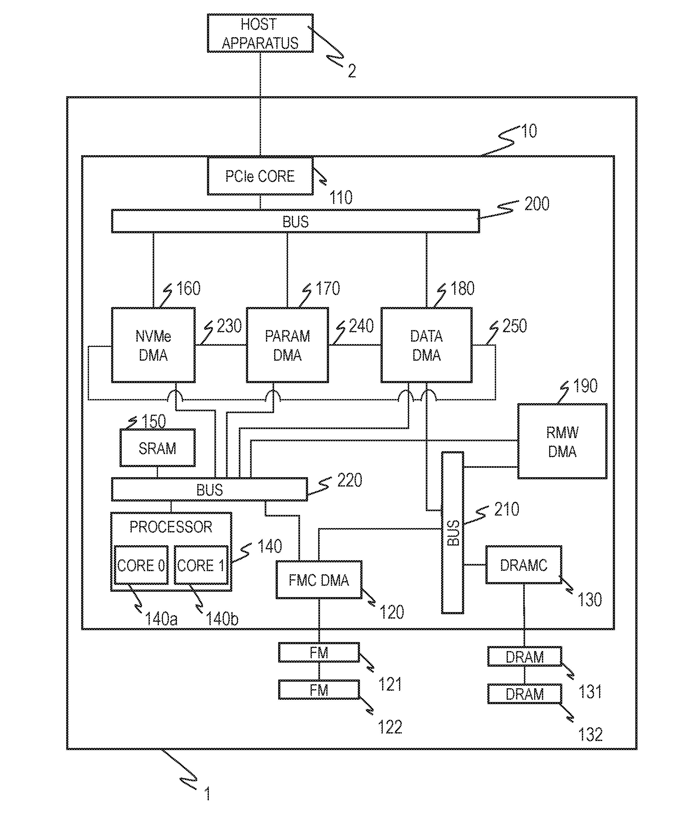
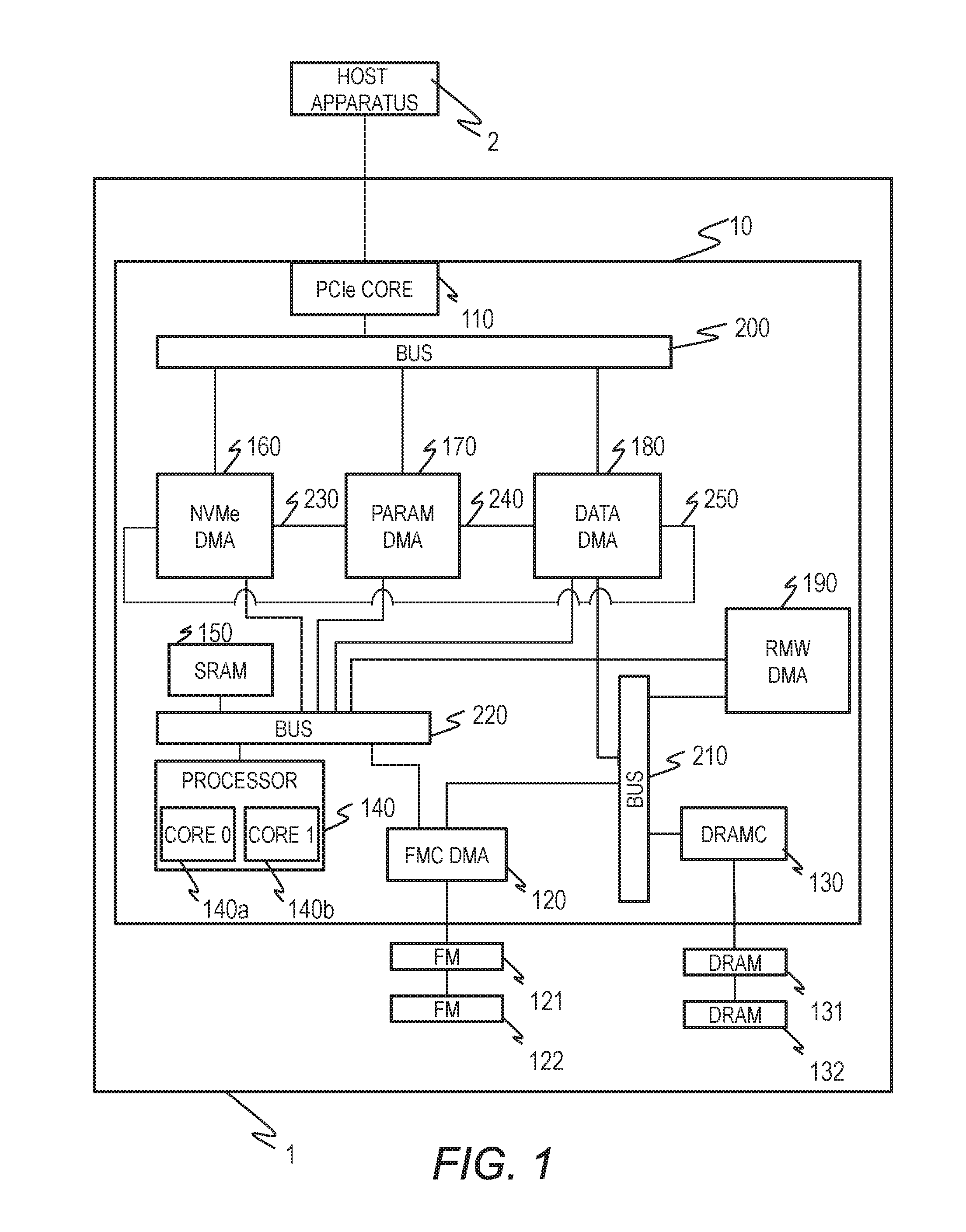
[0042]FIG. 1 is a block diagram for illustrating the configuration of a cache device in this embodiment. A cache device 1 is used while being coupled to a host apparatus 2 via a PCI-Express (PCIe) bus. The host apparatus 2 uses command sets of the NVMe protocol to input / output generated data and data received from other apparatus and devices. Examples of the host apparatus 2 include a server system and a storage system (disk array) controller. The host apparatus 2 can also be phrased as an apparatus external to the cache device.

[0043]The cache device 1 includes hardware logic 10, which is mounted as an LSI or an FGPA, flash memory chips (FMs) 121 and 122, which are used as storage media of the cache device 1, and dynamic random access memories (DRAMs) 131 and 132, which are used as temporary storage areas. The FMs 121 and 122 and the DRAMs 131 and 132 may be replaced by other combinations as long as d...

second embodiment

[0158]In the first embodiment, the basic I / O operation of the cache device 1 in this invention has been described.

[0159]The second embodiment describes cooperation between the cache device 1 and a storage controller, which is equivalent to the host apparatus 2 in the first embodiment, in processing of compressing data to be stored in an HDD, and also describes effects of the configuration of this invention.

[0160]The cache device 1 in this embodiment includes a post-compression size in notification information for notifying the completion of reception of write data to the processor 140 (S9460 of FIG. 9). The cache device 1 also has a function of notifying, at an arbitrary point in time, to the processor 140, the post-compression size of an LBA range about which an inquiry has been received.

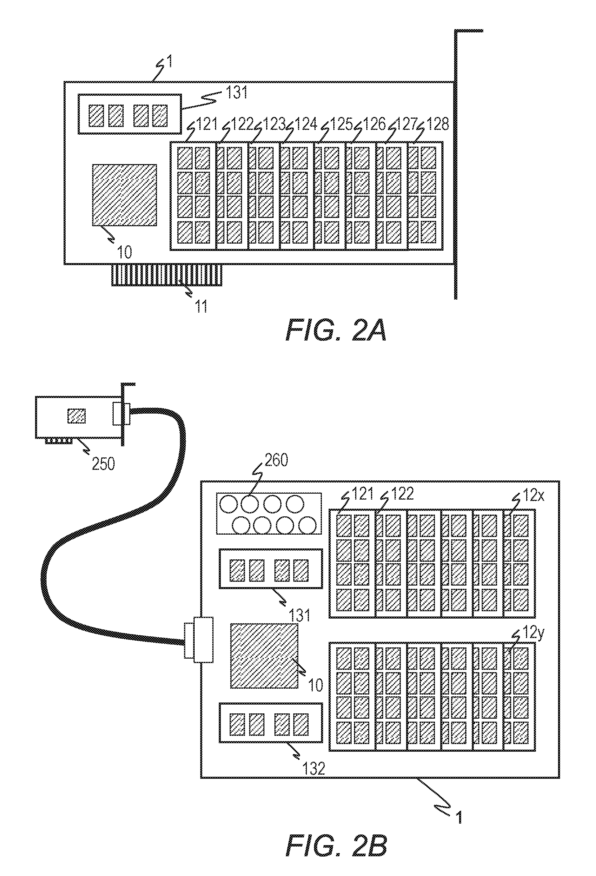
[0161]FIG. 13 is a block diagram for illustrating the configuration of a PCIe-connection cache device that is mounted in a storage device in this invention.

[0162]A storage device 13 is a device tha...


PUM


Abstract

A data memory device has a command transfer direct memory access (DMA) engine configured to obtain a command that is generated by an external apparatus to give a data transfer instruction from a memory of the external apparatus; obtain specifics of the instruction; store the command in a command buffer; obtain a command number that identifies the command being processed; and activate a transfer list generating DMA engine by transmitting the command number depending on the specifics of the instruction of the command. The transfer list generating DMA engine is configured to: identify, based on the command stored in the command buffer, an address in the memory to be transferred between the external apparatus and the data memory device; and activate the data transfer DMA engine by transmitting the address to the data transfer DMA engine which then transfers the data to / from the memory based on the received address.

Description

BACKGROUND OF THE INVENTION[0001]This invention relates to a PCIe connection-type data memory device.[0002]Computers and storage systems in recent years require a memory area of large capacity for fast analysis and fast I / O processing of a large amount of data. An example thereof in computers is in-memory DBs and other similar types of application software. However, the capacity of a DRAM that can be installed in an apparatus is limited for cost reasons and electrical mounting constraints. As an interim solution, NAND flash memories and other semiconductor storage media that are slower than DRAMs but faster than HDDs are beginning to be used in some instances.[0003]Semiconductor storage media of this type are called solid state disks (SSDs) and, as “disk” in the name indicates, have been used by being coupled to a computer or a storage controller via disc I / O interface connection by a serial ATA (SATA) or a serial attached SCSI (SAS) and via a protocol therefore.[0004]Access via the...

Claims


Application Information

Patent Timeline
Patent Type & Authority Applications(United States)
IPC IPC(8): G06F13/28G06F11/07G06F13/16G06F13/42G06F3/06G06F12/0868
CPCG06F13/28G06F2213/0026G06F3/0656G06F3/0659G06F3/0638G06F3/0689G06F3/0683G06F12/0868G06F13/1673G06F13/4282G06F11/0727G06F11/0751G06F11/0772G06F2212/1016G06F3/061G06F2212/401
Inventor ARAI, MASAHIROSUZUKI, AKIFUMIOKADA, MITSUHIROITO, YUJIHIRONAKA, KAZUEIMORISHITA, SATOSHISHIMOZONO, NORIO
Owner HITACHI LTD
Why Eureka
Try Eureka