Grating Element and External-Resonator-Type Light Emitting Device

Active Publication Date: 2016-11-24
NGK INSULATORS LTD
View PDF4 Cites 2 Cited by
  • Summary
  • Abstract
  • Description
  • Claims
  • Application Information

AI Technical Summary

Benefits of technology

[0049]Then, ΔλG can be made 0.8 nm or more and 6 nm or less by adjusting the depth td of the grooves that constitute a Bragg grating within a range of 20 nm or more and 250 nm or less, and the number of the longitudinal modes within the ΔλG can be adjusted within a range of from 2 to 5. Thus, the wavelengths satisfying the phase condition are discrete. When the number

Problems solved by technology

Particularly as the current and the temperature changes, the laser oscil

Method used


Image

  • Grating Element and External-Resonator-Type Light Emitting Device
  • Grating Element and External-Resonator-Type Light Emitting Device
  • Grating Element and External-Resonator-Type Light Emitting Device

Examples


example 1

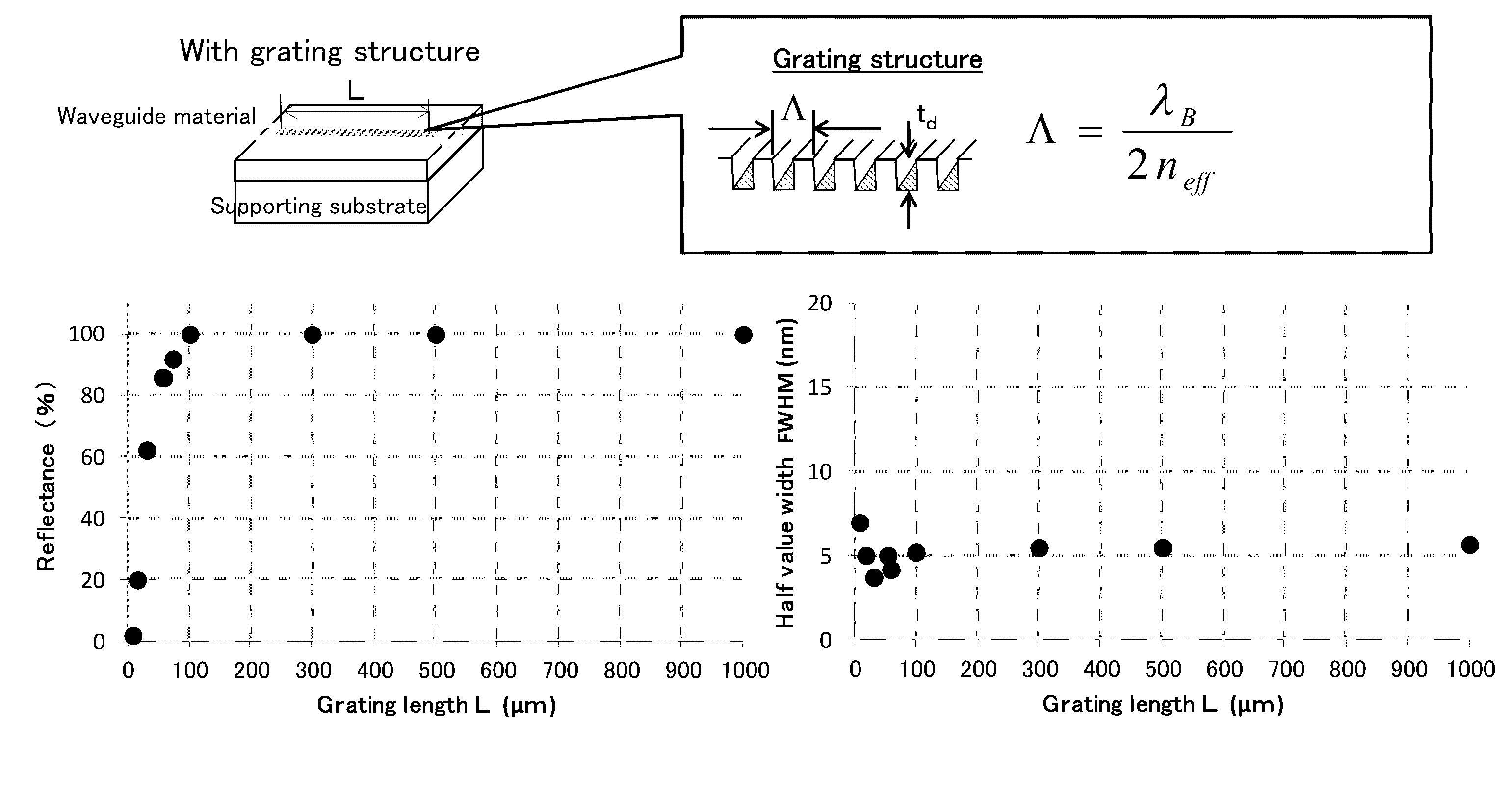
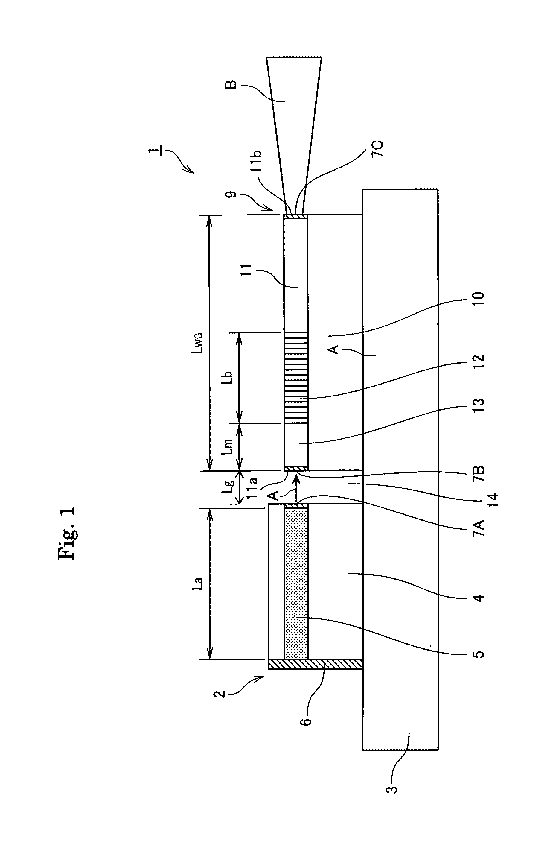
[0160]The device 9 as illustrated in FIG. 1 and FIG. 2 was produced.

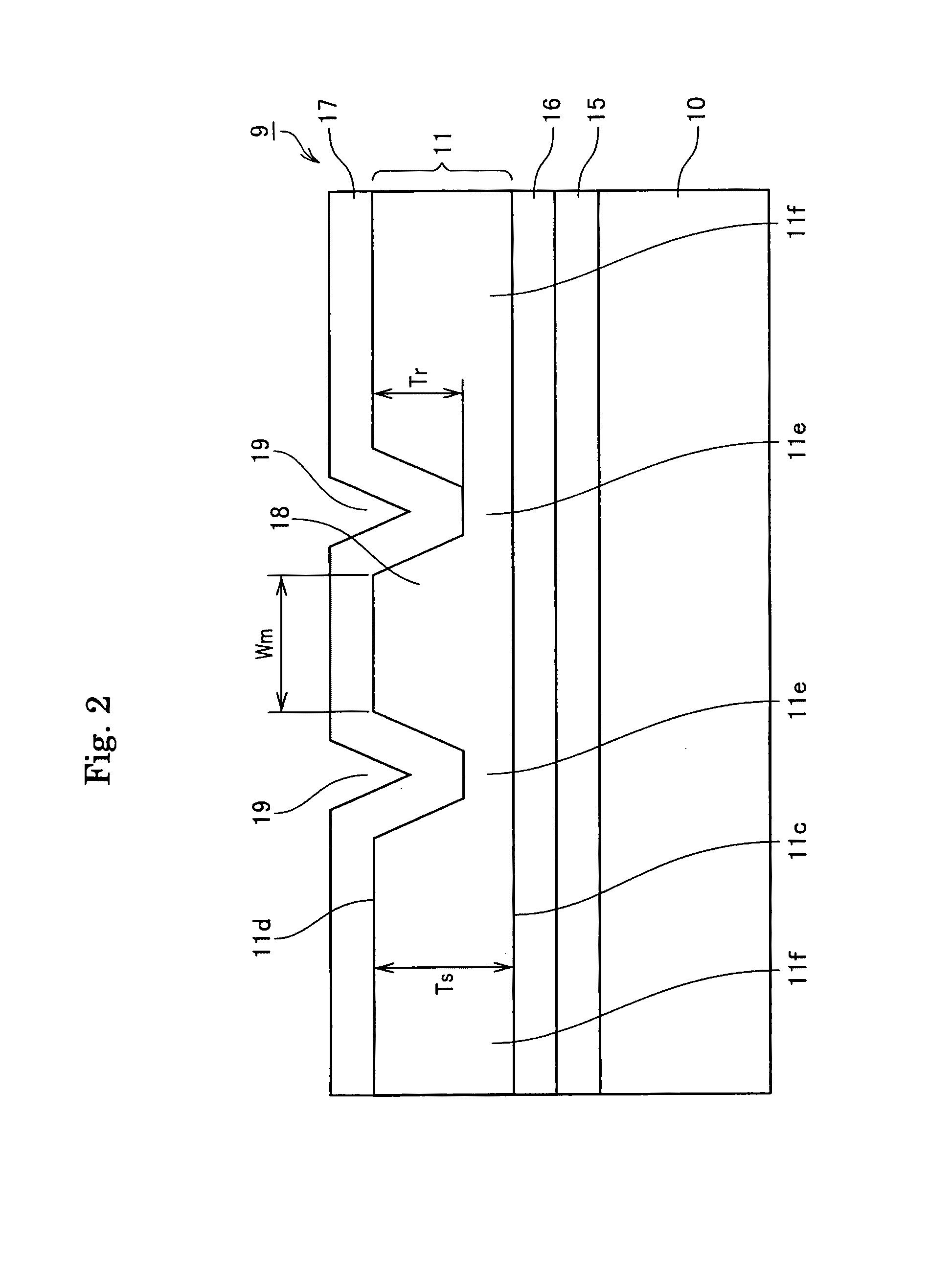
[0161]In particular, Ta2O5 was deposited at a thickness of 1.2 μm on a quartz substrate using a sputtering device to form a waveguide layer. Then, Ti was deposited on the Ta2O5, and a grating pattern was formed along the y-axis by photolithography. Then, grating grooves having a pitch spacing Λ of 232 nm and a length Lb of from 5 to 100 μm, 300 μm, 500 μm, or 1000 μm were formed using the Ti pattern as a mask by reactive ion etching with fluorine based gases. The grating had a groove depth td of 20, 40, 60, 100, 160, 200, or 350 nm. To form an optical waveguide that causes light to propagate along the y-axis, grooves having a width Wm of 3 μm and Tr of 0.5 μm were formed by reactive ion etching in a manner similar to the manner described above.

[0162]Then, the resultant was cut into bars using a dicing device. The both end faces were optically polished, and then an AR coating having a reflectance of 0.1% was coated o...

example 2

[0168]Ti was deposited on a substrate of z-cut lithium niobate crystal doped with MgO, and a grating pattern was formed along the y-axis by photolithography. Then, grating grooves having a pitch spacing Λ of 214 nm and a length Lb of 100 μm were formed using the Ti pattern as a mask by reactive ion etching with fluorine based gases. The grating had a groove depth of 20, 40, or 60 nm. To form an optical waveguide that causes light to propagate along the y-axis, grooves were formed in the grating by eximer laser so as to provide a width Wm of 3 μm and Tr of 0.5 μm. On the surface having the grooves formed therein, a buffer layer 16 of SiO2 was deposited at a thickness of 0.5 μm using a sputtering device. A black LN substrate, which was used as a support substrate, was bonded to the surface having the grating formed thereon.

[0169]Then, the resultant was attached to a polishing surface plate with the black LN substrate facing the surface plate, and the back side of the LN substrate havi...

example 3

[0175]Ti was deposited on a y-cut lithium niobate crystal substrate doped with MgO, and a grating pattern was formed along the x-axis by photolithography. Then, grating grooves having a pitch spacing Λ of 224 nm and a length Lb of 100 μm were formed using the Ti pattern as a mask by reactive ion etching with fluorine based gases. The grating had a groove depth of 20, 40, or 60 nm. To form an optical waveguide that causes light to propagate along the x-axis, grooves were formed in the grating by eximer laser so as to provide a width Wm of 3 μm and Tr of 0.5 μm. And on the surface having the grooves formed therein, a buffer layer 16 of SiO2 was deposited at a thickness of 0.5 μm using a sputtering device. A black LN substrate, which was used as a support substrate, was bonded to the surface having the grating formed thereon.

[0176]Then, the resultant was attached to a polishing platen with the black LN substrate facing the platen, and the back side of the LN substrate having the gratin...


PUM


Abstract

A grating device includes a support substrate, an optical material layer 11 disposed on the support substrate and having a thickness of 0.5 μm or more and 3.0 μm or less, a ridge optical waveguide formed by a pair of ridge grooves in the optical material layer and having a light-receiving surface for receiving a semiconductor laser light and a light-emitting surface for emitting light having a desired wavelength, a Bragg grating 12 comprising convexes and concaves formed in the ridge optical waveguide, and a propagating portion 13 disposed between the light-receiving surface and the Bragg grating. The relationships represented by the following Formulas (1) to (4) are satisfied:
0.8 nm≦ΔλG≦6.0 nm  (1);
10 μm≦Lb≦300 μm  (2);
20 nm≦td≦250 nm  (3); and
nb≧1.8  (4).

Description

TECHNICAL FIELD[0001]The present invention relates to a grating device and an external resonator type light emitting system that uses the grating device.BACKGROUND ARTS[0002]Generally, semiconductor lasers having Fabry-Perot (FP) resonator configuration are used, the resonator being formed by mirrors on the both end faces of an active layer. However, the FP lasers produce laser light at a wavelength that satisfies conditions for forming standing waves. Thus, the lasers tend to operate in a multi-longitudinal mode. Particularly as the current and the temperature changes, the laser oscillation wavelength varies, which results in a change in optical intensity.[0003]Thus, in applications in optical communication, gas sensing, and the like, there has been a need for a laser that exhibits high wavelength stability and that operates in a single mode. Thus, distributed feed-back (DFB) lasers and distributed reflection (DBR) lasers have been developed. These lasers include a grating in a sem...

Claims


Application Information

Patent Timeline
IPC IPC(8): H01S5/14
CPCH01S5/141G02B5/1814G02B6/124H01S5/02415H01S5/0287H01S5/0654H01S5/146H01S5/22H01S2301/163H01S5/14
Inventor KONDO, JUNGOYAMAGUCHI, SHOICHIROEJIRI, TETSUYAASAI, KEIICHIROOKADA, NAOTAKE
Owner NGK INSULATORS LTD
Why Eureka
Try Eureka