Reverse conducting IGBT

a reverse recovery and igbt technology, applied in the field of reverse conducting igbt, can solve the problems of deterioration of faulty electrical connection, and achieve the effects of reducing power loss in the igbt structure, improving the reverse recovery characteristics of the diode structure, and increasing the carrier concentration

Active Publication Date: 2016-12-01
DENSO CORP
View PDF0 Cites 33 Cited by
  • Summary
  • Abstract
  • Description
  • Claims
  • Application Information

AI Technical Summary

Benefits of technology

[0010]In the reverse conducting IGBT according to the above-mentioned aspect, the trench gate member in the IGBT region has the lattice-pattern layout, and the trench member in the diode region has the stripe-pattern layout. Since the trench gate member in the IGBT region has the lattice-pattern layout, there is an increase in carrier concentration of the IGBT region, and thus there is a reduction in power loss in the IGBT structure. Meanwhile, the trench member in the diode region includes the plurality of stripe trenches extending along the first direction. For this reason, the bather region provided in the diode region is not divided by the trench member in the first direction and can thus spread over a wide area along the first direction. Therefore, as long as some part of the bather region extending over a wide area in the first direction can be surely electrically connected to the top surface electrode via the pillar member, the whole of the barrier region is electrically connected to the top surface electrode. This enables the barrier region to reduce the number of holes injected from the anode region into the drift region and thus improve reverse recovery characteristics of the diode structure. Thus, the reverse conducting IGBT according to the aspect, in which the trench gate member in the IGBT region and the trench member in the diode region have different layout, can achieve both a reduction in power loss in the IGBT region and improvement in the reverse recovery characteristics of the diode structure.

Problems solved by technology

It has become obvious that if, in this case, the trench member in the diode region is configured, in consideration of symmetry, to also have a lattice-pattern layout, the following problems arise.
However, if there is a malformation in a pillar member that corresponds to any of the parts into which the barrier region has been divided, there is a faulty electrical connection between that pillar member and the emitter electrode.
This disables that part of the barrier region which corresponds to the pillar region, thus giving rise to deterioration in the reverse recovery characteristics of the diode structure.

Method used


Image

  • Reverse conducting IGBT
  • Reverse conducting IGBT
  • Reverse conducting IGBT

Examples


Embodiment Construction

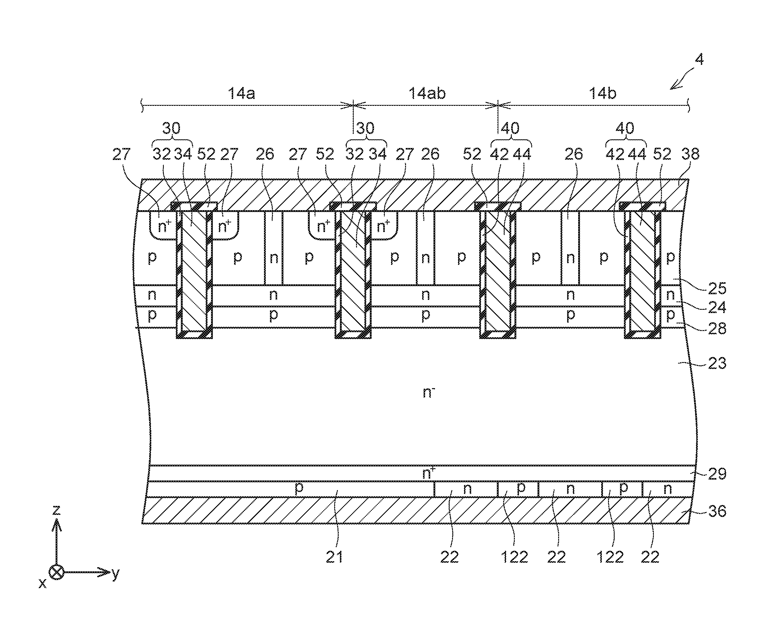
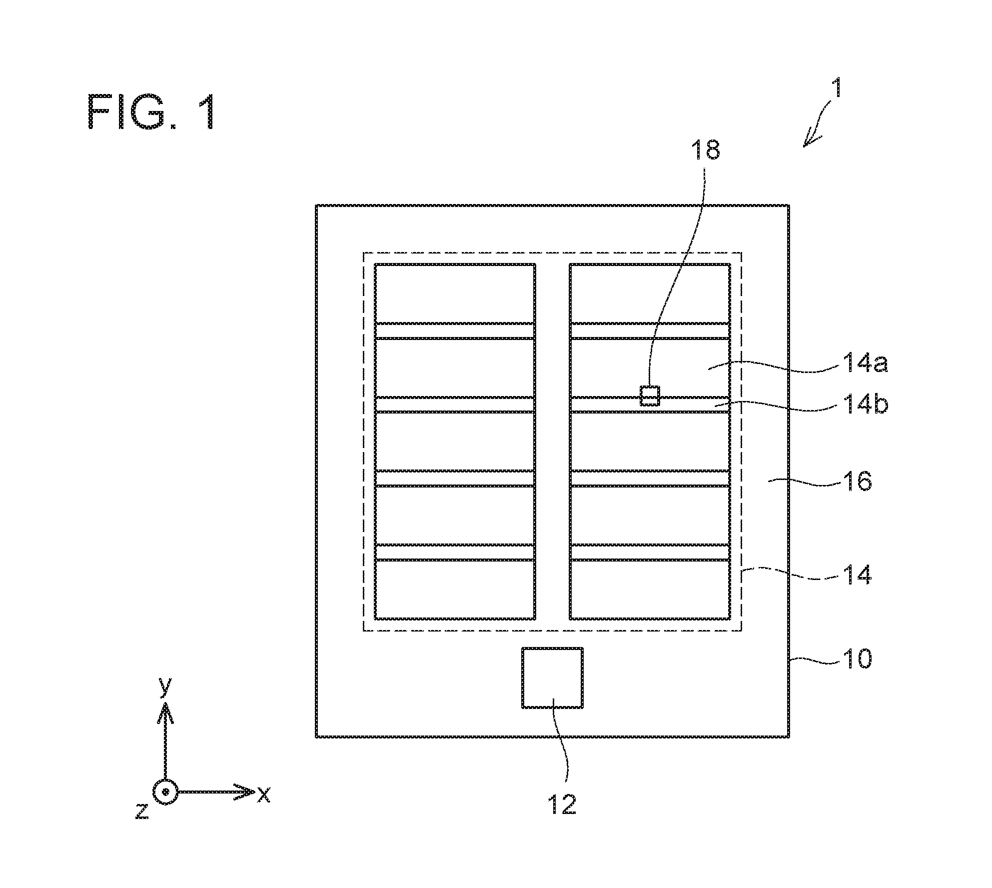
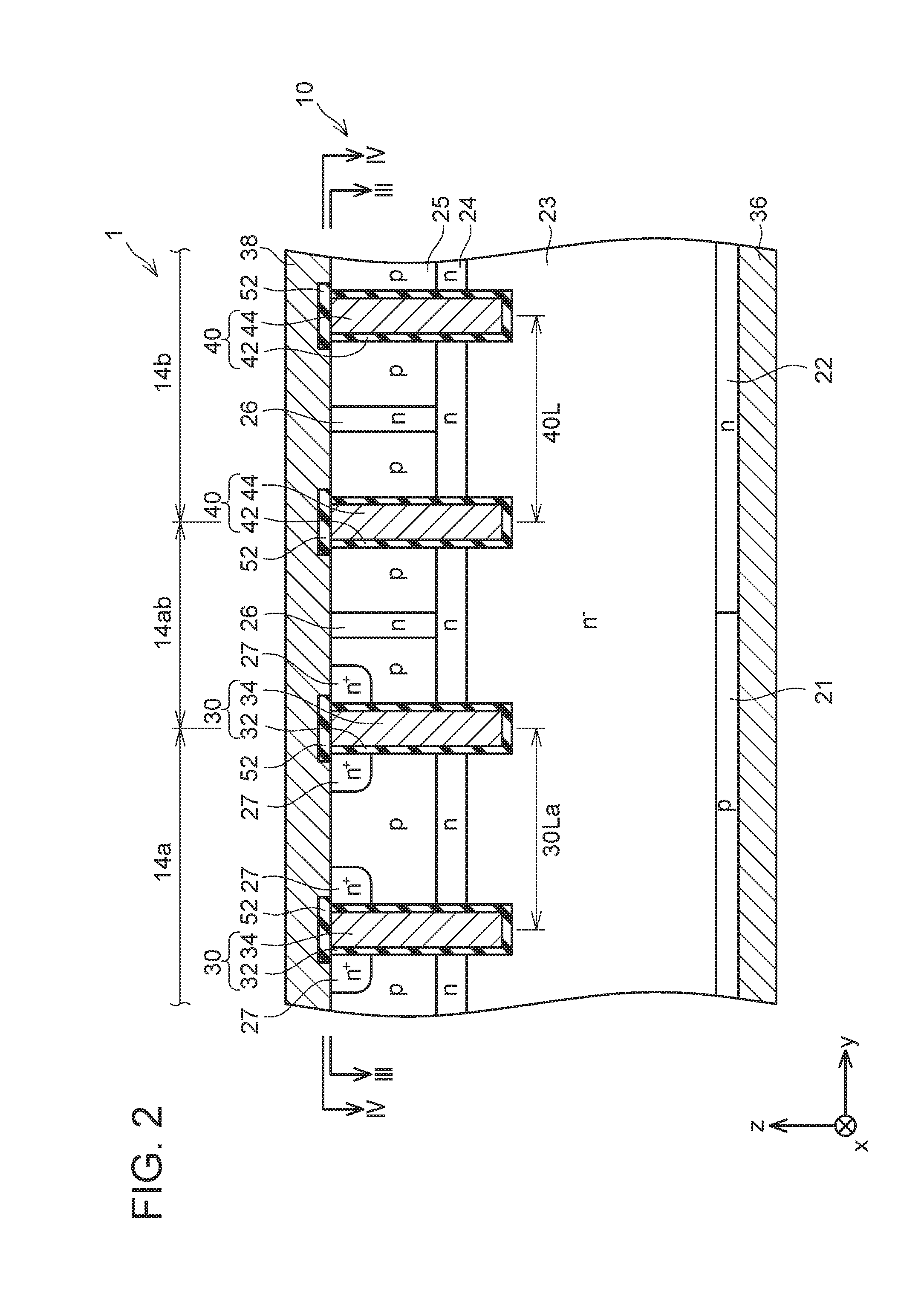
[0028]As shown in FIG. 1, a reverse conducting IGBT 1 includes a semiconductor substrate 10 partitioned into an element portion 14 and a terminal portion 16. In one example, the semiconductor substrate 10 is an n−-type Si single-crystal. substrate having a specific resistance of 40 to 100 Ωcm and a thickness of 80 to 165 μm. The element portion 14, which is partitioned on a center side of the semiconductor substrate 10, is a portion in which a current flows in a thickness direction (z-axis direction), and is provided with IGBT and diode structures to be described later. The terminal portion 16, which is partitioned on a peripheral side of the semiconductor substrate 10, is a portion that relaxes an electric field on the peripheral side of the semiconductor substrate 10, and is provided with a withstand-voltage structure such as a guard ring. Further provided on the terminal portion 16 of the semiconductor substrate 10 is a gate pad 12. Connected to this gate pad 12 is a gate wire (n...


PUM


Abstract

A reverse conducting IGBT is provided with a trench gate member that is provided in an IGBT region and has a lattice-pattern layout, and a trench member that is provided in a diode region and has a stripe-pattern layout. The diode region of the semiconductor substrate includes an anode region of a first conductive type, a drift region of a second conductive type and a barrier region of the second conductive type. The barrier region is electrically connected to a top surface electrode via a pillar member that extends from a top surface of the semiconductor substrate.

Description

CROSS-REFERENCE TO RELATED APPLICATION[0001]This application claims priority to Japanese Patent Application No. 2015407314 filed on May 27, 2015, the contents of which are hereby incorporated by reference into the present application.TECHNICAL FIELD[0002]The technique disclosed in the present application relates to a reverse conducting IGBT (Insulated Gate Bipolar Transistor).DESCRIPTION OF RELATED ART[0003]For example, reverse conducting IGBTs have been under development for use as on-vehicle power devices. A reverse conducting IGBT includes a semiconductor substrate partitioned into an IGBT region in which an IGBT structure is provided and a diode region in which a diode structure is provided. The diode structure is connected in antiparallel to the IGBT structure, and. functions as a free-wheeling diode.[0004]Japanese Patent Application Publication No. 2013-48230 (FIGS. 16 to 17 and 47 to 50 in particular) discloses a reverse conducting IGBT having an n-type barrier region provide...

Claims


Application Information

Patent Timeline
Patent Type & Authority Applications(United States)
IPC IPC(8): H01L27/06H01L29/739H01L29/06H01L29/872
CPCH01L27/0635H01L29/872H01L29/0696H01L29/0684H01L29/7397H01L29/7393H01L29/407H01L29/0603H01L29/0619H01L29/0692H01L27/0727H01L29/4238H01L29/0834H01L29/1095H01L29/4236H01L29/6609H01L29/66325H01L29/66734
Inventor SENOO, MASARU
Owner DENSO CORP
Why Eureka
Try Eureka