

Scanning Electron Microscope System, Pattern Measurement Method Using Same, and Scanning Electron Microscope
a scanning electron microscope and scanning electron microscope technology, applied in semiconductor/solid-state device testing/measurement, instruments, nuclear engineering, etc., can solve the problem of reducing the merit of the cost obtained by reducing the chip area by lithography and the increase of manufacturing costs
- Summary
- Abstract
- Description
- Claims
- Application Information
AI Technical Summary
Benefits of technology
Problems solved by technology
Method used
Image

Examples
first embodiment
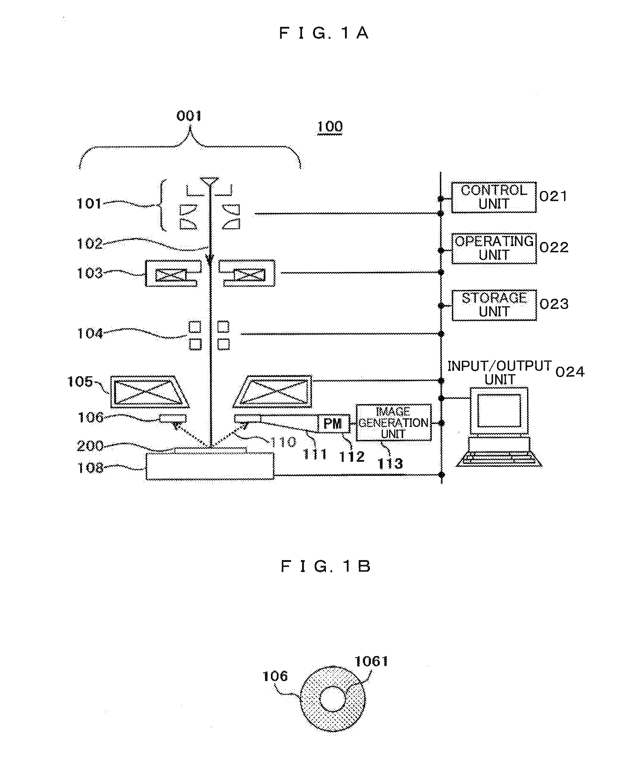
[0064]FIG. 1A is the basic configuration of a scanning electron microscope system 100 to which the present invention is applied. The electron microscope system 100 is configured of an imaging optical system 001, a control unit 021, an operating unit 022, a storage unit 023, an input / output unit 024, and other components. The imaging optical system 001 generates a primary electron beam 102 at a high accelerating voltage (e.g. a voltage of 30 kV or more) from an electron gun 101, focuses the primary electron beam 102 at a capacitor lens 103, passes the primary electron beam 102 through an objective lens 105, and then focuses the primary electron beam 102 on the surface of a sample 200.
[0065]The primary electron beam 102 is two-dimensionally scanned over the sample 200 by a deflector 104. Backscattered electrons 110 in a low angle direction emitted from the sample 200 are received at an annular yttrium aluminium garnet (YAG) scintillator 106 (see FIG. 1B), and converted into optical si...
second embodiment
[0077]In this embodiment, a method is provided for measuring the diameter of a hole as well as the depth of a hole.
[0078]The present invention implements the observation of the bottom of a hole by detecting BSEs having penetrated the side wall. However, a deep hole with a large aspect ratio prolongs a distance required for electrons having been emitted from the bottom of the hole to penetrate the side wall and reach the surface. Thus, the ratio of electrons that consume energy in the midway and fail to penetrate the surface is increased. In other words, on the obtained image, the depth of a hole can be measured (estimated) using the relationship in which a deeper hole has a darker hole part.
[0079]In the following, in order to implement the measurement of the depth of a hole, necessary conditions for the configuration will be shown. The configuration of a scanning electron microscope system used in the embodiment is the same as the configuration of the scanning electron microscope sy...
third embodiment
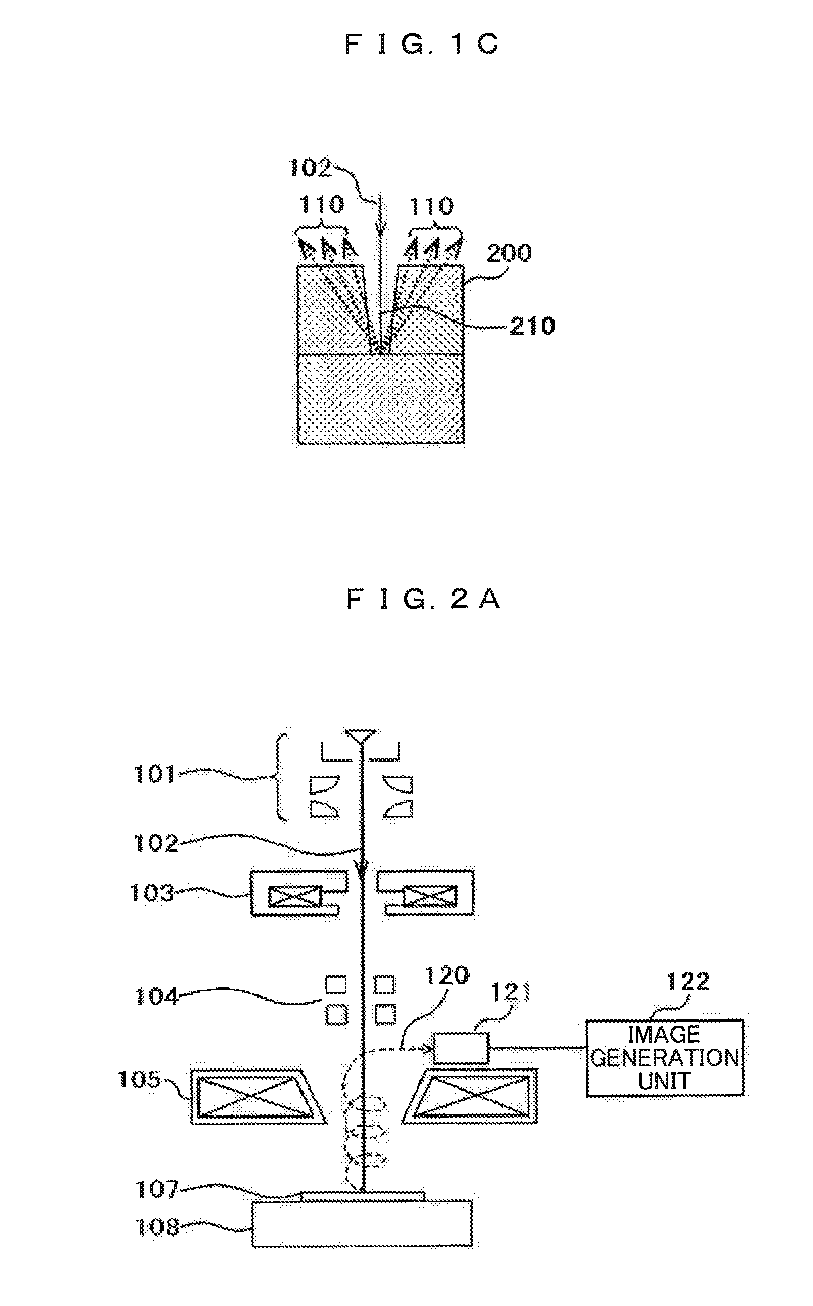
[0093]FIG. 11A is the basic configuration of an imaging optical system 002 according to a third embodiment of the present invention. The difference from the imaging optical system 001 described in the first embodiment (see FIG. 1A) lies in that a detector 121 that detects secondary electrons 120 emitted from a sample 200 is additionally provided.
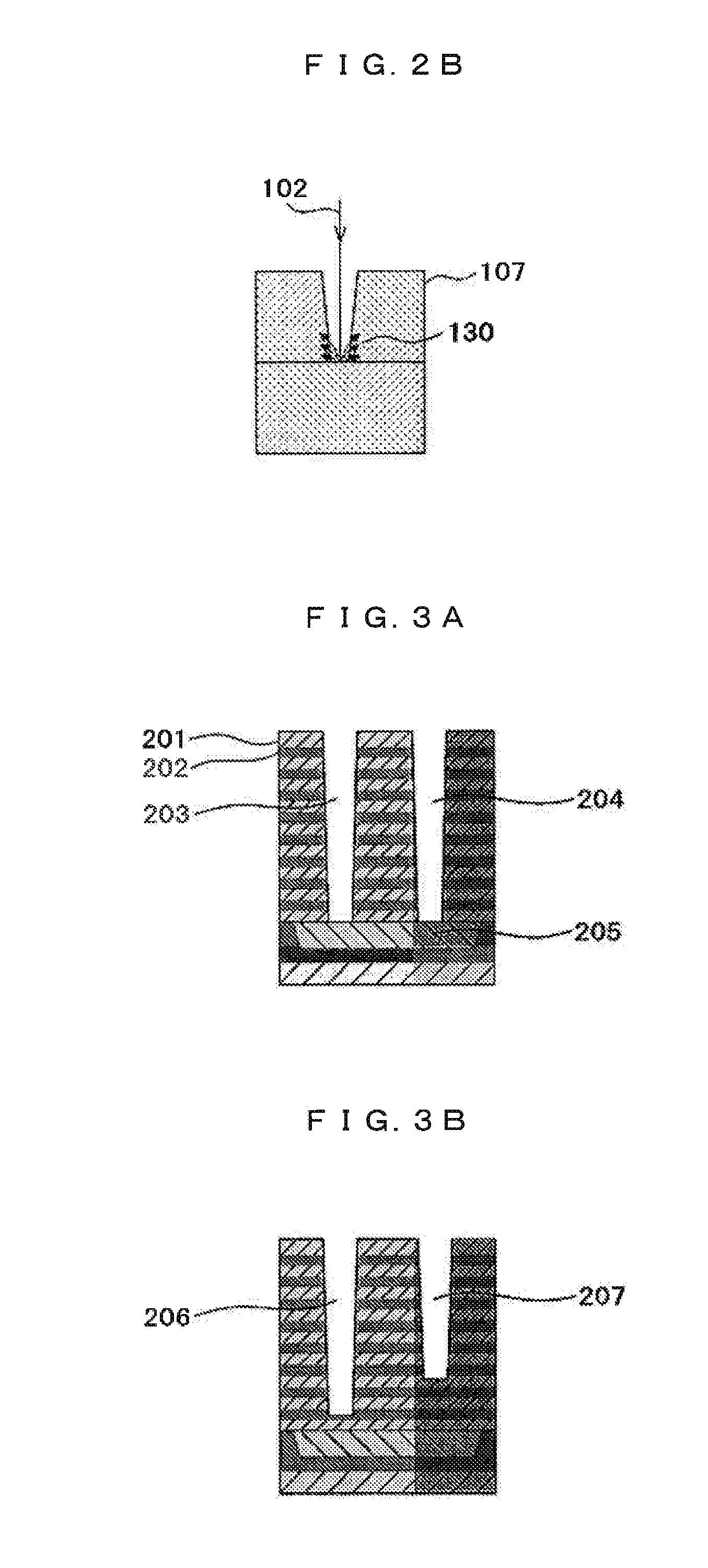
[0094]As illustrated in FIG. 2B, or FIGS. 4C and 4D, secondary electrons (SEs) emitted from the bottom of a hole formed on the sample fail to escape to the hole outer region. However, as illustrated in FIG. 11B, secondary electrons 130 emitted from near a top edge 131 of the hole are detected at the detector 121.
[0095]As the schematic diagram 1310 illustrated in FIG. 12A, secondary electrons (130 in FIG. 11B) emitted from near a top edge 1312 of a hole 1311 have a bright peak on the image by the edge effect. Thus, these electrons are suited to the measurement of the top diameter of a hole. As illustrated in FIG. 12B, the detection of peaks 1...
PUM
 Abstract
Description
Claims
Application Information