Fabric interconnection for memory banks based on network-on-chip methodology

a technology of memory banks and network on chips, applied in the field of data storage systems, can solve the problems of excessive amount, inability of memory technologies to address the current and future capacity demands of next-generation computing systems, and the amount of wires needed to route the entire memory, etc., to achieve unlimited memory density growth, reduce parasitic capacitance and resistance, and reduce latencies between matrices

Active Publication Date: 2017-04-27
WESTERN DIGITAL TECH INC
View PDF15 Cites 24 Cited by
  • Summary
  • Abstract
  • Description
  • Claims
  • Application Information

AI Technical Summary

Benefits of technology

[0009]Embodiments disclosed herein generally relate to the use of Network-on-Chip architecture for solid state memory structures, both volatile and non-volatile, which provide for the access of memory storage blocks via a router. As such, data may be sent to and / or from the memory storage blocks as data packets on the chip. The Network-on-Chip architecture may further be utilized to interconnect unlimited numbers of memory cell matrices, spread on a die, thus allowing for reduced latencies among matrices, selective power control, unlimited memory density growth without major latency penalties, and reduced parasitic capacitance and resistance. Other benefits may include improved signal integrity, larger die areas available to implement memory arrays, and higher frequency of operation.

Problems solved by technology

Today the memory technologies that generally dominate the computing industry are DRAM and NAND flash; however, these memory technologies may not be able to address the current and future capacity demands of next generation computing systems.
As such, the biggest limitation with existing memory bank architecture is the amount of wire necessary to route the entire memory.
Excessive amount of wire is the main cause for latency in existing memory banks from SRAM to DRAM.
With such limitations, there may only be one physical access interface, due to complexity and cost, to implement additional interfaces.

Method used


Image

  • Fabric interconnection for memory banks based on network-on-chip methodology
  • Fabric interconnection for memory banks based on network-on-chip methodology
  • Fabric interconnection for memory banks based on network-on-chip methodology

Examples


Embodiment Construction

[0022]In the following disclosure, reference is made to embodiments. However, it should be understood that the disclosure is not limited to specific described embodiments. Instead, any combination of the following features and elements, whether related to different embodiments or not, is contemplated to implement and practice the claimed subject matter. Furthermore, although embodiments described herein may achieve advantages over other possible solutions and / or over the prior art, whether or not a particular advantage is achieved by a given embodiment is not limiting of the claimed subject matter. Thus, the following aspects, features, embodiments and advantages are merely illustrative and are not considered elements or limitations of the appended claims except where explicitly recited in a claim(s).

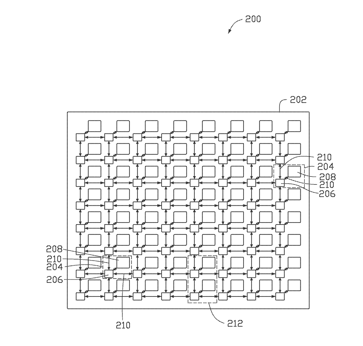
[0023]Embodiments disclosed herein generally relate to the use of Network-on-Chip architecture for solid-state memory structures that provide for the access of memory storage blocks via...


PUM


Abstract

Embodiments disclosed herein generally relate to the use of Network-on-Chip architecture for solid state memory structures, both volatile and non-volatile, which provide for the access of memory storage blocks via a router. As such, data may be sent to and/or from the memory storage blocks as data packets on the chip. The Network-on-Chip architecture may further be utilized to interconnect unlimited numbers of memory cell matrices, spread on a die, thus allowing for reduced latencies among matrices, selective power control, unlimited memory density growth without major latency penalties, and reduced parasitic capacitance and resistance. Other benefits may include improved signal integrity, larger die areas available to implement memory arrays, and higher frequency of operation.

Description

BACKGROUND[0001]Field[0002]Embodiments disclosed herein generally relate to data storage systems, and more particularly, to a memory device utilizing Network-on-Chip architecture for the interconnection of memory subarrays, mats, arrays, subbanks, and / or banks[0003]Description of the Related Art[0004]The cerebral cortex of a computer is a magnetic recording device, which typically may include a rotating magnetic media or a solid state media device. A number of different memory technologies exist today for storing information for use in a computing system.[0005]In recent years, there has been a demand for higher density devices, which maintain a relatively low cost per bit, for use in high capacity storage applications. Today the memory technologies that generally dominate the computing industry are DRAM and NAND flash; however, these memory technologies may not be able to address the current and future capacity demands of next generation computing systems.[0006]Existing non-volatile...

Claims


Application Information

Patent Timeline
Patent Type & Authority Applications(United States)
IPC IPC(8): H04L12/933G06F3/06H04L45/24H04L45/74
CPCH04L49/109G06F3/067G06F3/0647G06F3/0604G06F13/1647G06F13/1657G06F13/1684H04L45/74H04L45/22H04L25/0264
Inventor BANDIC, ZVONIMIR Z.CARGNINI, LUISVUCINIC, DEJAN
Owner WESTERN DIGITAL TECH INC
Why Eureka
Try Eureka