Dielectric composite material for fingerprint sensor induction layer and preparation method thereof

a fingerprint sensor and composite material technology, applied in the field of dielectric composite materials for fingerprint sensor induction layer, can solve the problems of reducing the electric field intensity, the fingerprint of the user cannot be accurately read, and the sensing precision of the sensor becomes worse, and achieves the effect of high manufacturing cos

Inactive Publication Date: 2017-05-04
TECORE SYNCHEM
View PDF5 Cites 9 Cited by
  • Summary
  • Abstract
  • Description
  • Claims
  • Application Information

AI Technical Summary

Benefits of technology

[0007]Besides the IC encapsulation process, the lens-encapsulated fingerprint sensor needs additional encapsulation steps such as a pre-cutting step and

Problems solved by technology

In order to guarantee the precision of the sensor, the distance between a finger of the user and the surface of the silicon wafer cannot be too far; and when the distance between the finger and the surface of the silicon wafer is increased, the electric field intensity is decreased, the sensing precision of the sensor becomes worse, and the fingerprint of the user cannot be accurately read.
However, subjected to the limitation of a processing method (a chemical vapor deposition (CVD) method is often used), the thickness of the protection thin layer is generally only hundreds of nanometers to 4 micrometers and cannot be more than 10 micrometer

Method used


Image

  • Dielectric composite material for fingerprint sensor induction layer and preparation method thereof
  • Dielectric composite material for fingerprint sensor induction layer and preparation method thereof
  • Dielectric composite material for fingerprint sensor induction layer and preparation method thereof

Examples


embodiment 1-1

[0084]Preparation of the Dielectric Composite Material for the Fingerprint Sensor Induction Layer.

[0085]a small-batch preparation method of the dielectric composite material:

[0086](1) raw materials are weighed according to embodiment 1;

[0087](2) the epoxy resin, the first type of dielectric inorganic filler, the second type of dielectric inorganic filler and the adhesive force accelerant are mixed by a two-roll rubber mixing mill for 0.5 hour under the condition of 150° C., and then the releasing agent and the fire retardant are added and mixed for 1 minute; the temperature is adjusted to 80° C., and the phenolic resin and a catalyst are added, mixed uniformly for 10 minutes and then extruded into sheets, the sheets are cooled to a room temperature, crushed and compacted into tablets to obtain the dielectric composite material for the fingerprint sensor induction layer, and the dielectric composite material is stored in a refrigerator at a temperature less than 0 for standby use.

[00...

embodiment 40

[0092]An Application Method of a Dielectric Composite Material for a Fingerprint Sensor Induction Layer:

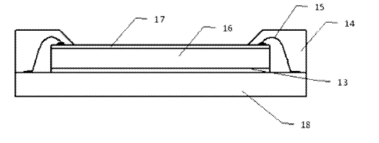
[0093]The dielectric composite material for the fingerprint sensor induction layer covers a fingerprint sensor chip through a high-temperature mold pressing molding method (molded in a hydraulic method), and the dielectric composite material for the fingerprint sensor induction layer is completely cured by means of heating curing, so that the fingerprint sensor chip can sense an electric signal on fingerprints so as to finally identify different fingerprint patterns, and the dielectric composite material can be well applied to the fingerprint sensor (refer to FIG. 1).

[0094]In FIG. 1, 1 is an encapsulation substrate; 2 is a sensor chip; 3 is a chip adhesive material; 4 is a bonding lead; and 5 is a dielectric composite material for the fingerprint sensor induction layer of the present invention.

embodiment 41

[0095]Table 3 properties of the dielectric composite material for the fingerprint sensor induction layer.

The dielectric compositeGelation time (t)material for the inductionmeasuredspiral followinglayer of the fingerprint temperaturelength (mm), measuredsensor prepared by table 2175° C.temperature 175° C.Embodiment 1-94273Embodiment 2-930120Embodiment 3-935110Embodiment 4-96065Embodiment 5-96555Embodiment 6-93565Embodiment 7-933140Embodiment 8-970100Embodiment 9-96085Embodiment 10-955153Embodiment 11-938120Embodiment 12-935110Embodiment 13-960130Embodiment 14-93094Embodiment 15-93788Embodiment 16-960110Embodiment 17-935140Embodiment 18-955120Embodiment 19-945150Embodiment 20-965135Embodiment 21-942120Embodiment 22-935140Embodiment 23-935110Embodiment 24-960155Embodiment 25-93095Embodiment 26-95595Embodiment 27-950100Embodiment 28-96095Embodiment 29-95585Embodiment 30-93080Embodiment 31-932105Embodiment 32-955120Embodiment 33-965110Embodiment 34-93060Embodiment 35-962120Embodiment 36-...


PUM

PropertyMeasurementUnit
Temperatureaaaaaaaaaa
Fractionaaaaaaaaaa
Fractionaaaaaaaaaa

Abstract

Provided is a dielectric composite material for a fingerprint sensor induction layer and a preparation method therefor, wherein the dielectric composite material is made from the following components: an epoxy resin, a phenolic resin, a first type of dielectric inorganic filler, a second type of dielectric inorganic filler, a curing agent, an adhesion promoter, a mould releasing agent and a flame retardant. The dielectric composite material has a high dielectric constant, a small dielectric loss, very stable dielectric properties which change very little with the test frequency, non-transparency and high hardness, such that the fingerprint sensor induction layer prepared therefrom satisfies the requirements of reliability and stability while reaching the thickness requirement, and can be used in various portable electronic products. The dielectric composite material for the fingerprint sensor induction layer is free of heavy metal lead, and is green and environmentally friendly. The dielectric composite material has convenience and high safety, and therefore the terminal application thereof can not only replace the existing digital-input password identification system, but can also be used on any electronic component in need of security.

Description

CROSS-REFERENCE TO RELATED APPLICATIONS[0001]This application is a continuation of International Patent Application No. PCT / CN2015 / 072993 with a filing date of Feb. 13, 2015, designating the United States, now pending, and further claims priority to Chinese Patent Application No. 201410437851.2 with a filing date of Aug. 29, 2014. The content of the aforementioned applications, including any intervening amendments thereto, are incorporated herein by reference.TECHNICAL FIELD[0002]The present invention relates to a dielectric composite material for a fingerprint sensor induction layer and a preparation method thereof.BACKGROUND OF THE PRESENT INVENTION[0003]At present, a typical encapsulation structure of a fingerprint sensor includes a silicon wafer on which an induction electrode and relevant circuits are formed. The fingerprint sensor (abbreviated as FPS) plays a role in sensing a relative distance between a ridge and a valley of finger skin of a user in a capacitive electric fiel...

Claims


Application Information

Patent Timeline
IPC IPC(8): C08L63/00G06K9/00C08L61/06
CPCC08L63/00C08L61/06G06K9/0002C08L2201/02B29C47/0004B29K2509/00B29K2063/00B29K2061/04B29K2105/0026B29K2995/0016B29K2995/0006B29C47/0038C04B26/14C04B2111/92C04B24/302C04B14/305C04B14/06C04B24/121C04B24/42C04B24/36C04B22/06C04B14/327C04B22/066C04B14/28C04B24/2611C04B22/064C08G59/50C08G59/621B29C48/001B29C48/022H01L2224/48465H01L2224/48091H01L2224/73265H01L2224/32225H01L2924/181H01L2224/48227G06V40/1329G06V40/1306C08K3/22C08K5/0066C08K5/54H01L2924/00014H01L2924/00012H01L2924/00
Inventor TAN, XIAOHUAHUO, JUYU, HUIYUNFENG, YAKAISUN, XUYUN
Owner TECORE SYNCHEM
Why Eureka
Try Eureka