
Use of heteroleptic indium hydroxides as precursors for inp nanocrystals

a technology of heteroleptic indium hydroxide and nanocrystals, applied in the field of nanostructure synthesis, can solve the problems of increasing production costs, affecting the ability of the one in the art to know and control, and the synthetic method will not produce consistent nanocrystal products

Active Publication Date: 2017-05-18
NANOSYS INC
View PDF0 Cites 7 Cited by
  • Summary
  • Abstract
  • Description
  • Claims
  • Application Information

AI Technical Summary

Benefits of technology

The present invention provides methods for preparing two compounds, namely, a compound of formula (I) and a compound of formula (III). These methods involve reacting specific precursors in a specific way to produce the desired compound. The compound of formula (I) is a compound of formula (O2CCH3)2OH(CH3)2O(CH2)bCH3(OH)c, wherein X1 is B, Al, Ga, In, or Tl and c is 1 or 2. The compound of formula (III) is a compound of formula (O2CCH3)2CH3(OH)c, wherein b is between 7 and 19 and c is 1 or 2. The methods involve specific reaction conditions, such as temperature and time, and specific solvents. The invention also provides a method for producing a Group III-V nanostructure by reacting a Group III precursor and a Group V precursor. The nanostructure can be used in various applications, such as electronics and optics.

Problems solved by technology

Because In(OAc)3 is both hydroscopic and moisture sensitive, it must be handled using inert atmosphere conditions requirements that increase production costs and require extensive purification of the other reagents used to remove any trace amounts of water.
Firstly, since the reagent used is a mixture, the synthetic method will not produce consistent nanocrystal products.
This is because a mixture will not allow one in the art to know and control the ratio of In3+ to long-chain carboxylic acid.
It is likely that In(O2C(CH2)mCH3)3-n(OH)n is not suitable for nanocrystal growth due to the high sensitivity of the reaction kinetics.
Thus, if In(O2C(CH2)mCH3)2(OH) and In(O2C(CH2)mCH3)3 react at different rates, the precursor conversion in nanocrystal growth—a step that is critical for obtaining a narrow size distribution—will be more difficult to control than when a single reaction material is used.

Method used


Image

  • Use of heteroleptic indium hydroxides as precursors for inp nanocrystals
  • Use of heteroleptic indium hydroxides as precursors for inp nanocrystals
  • Use of heteroleptic indium hydroxides as precursors for inp nanocrystals

Examples


example 1

Control Reaction for Preparation of In(O2CCH3)2OH

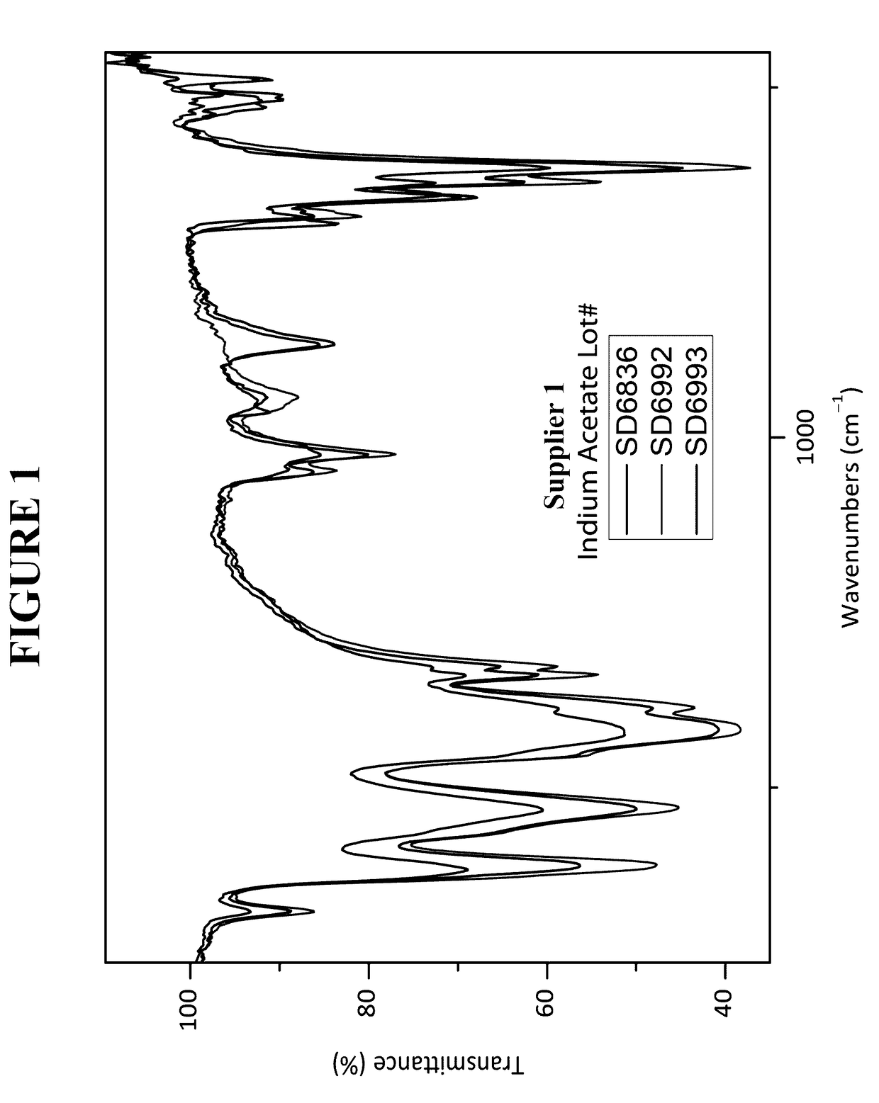
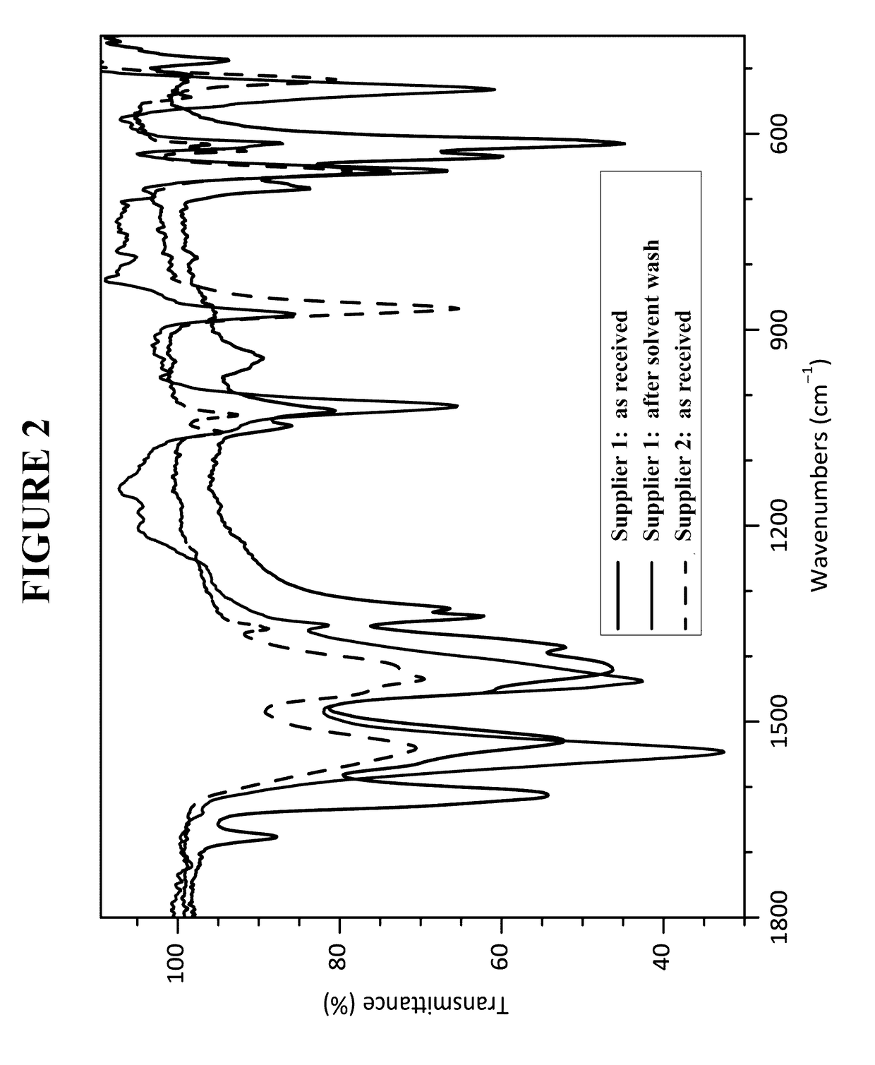
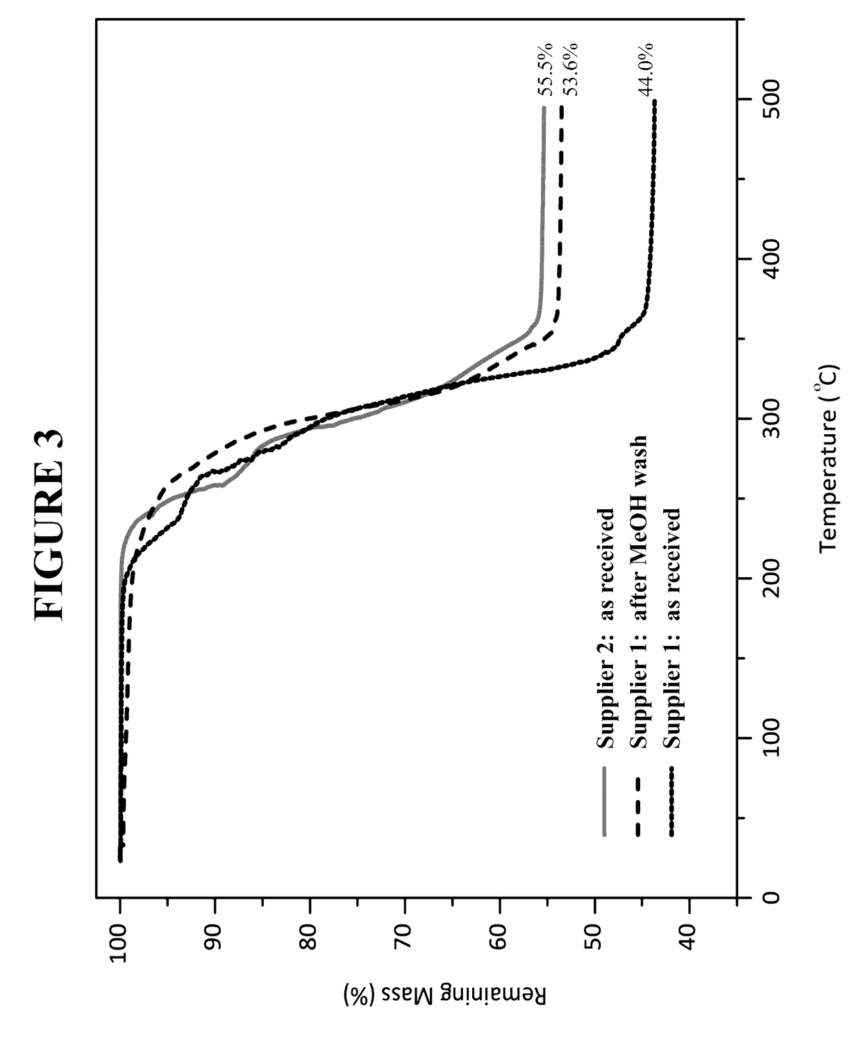
[0247]In the glovebox, three 500 mg samples (each from a different lot) of indium acetate (Indium Corporation, Utica, N.Y.) were weighed. To each sample was added 10 mL of anhydrous diethyl ether. The sample was vigorously shaken. Outside the glovebox, the samples were filtered through a M-porosity filtration / fritted funnel to collect the solids. In order to rinse the vials, hexanes were added and the slurry that formed was filtered. The solids were dried under dynamic vacuum for between 5 to 10 minutes. Each solid was analyzed by Fourier transform infrared spectroscopy (FTIR).

[0248]In the glovebox, three 500 mg samples of indium acetate (Indium Corporation, Utica, N.Y.) were weighed. To each sample was added 10 mL of anhydrous diethyl ether and 1 mL of deionized water. The samples were vigorously shaken. Outside the glovebox, the samples were filtered through a M-porosity filtration / fritted funnel to collect the solids. In order to r...

example 2

Synthesis of In(O2CCH3)2OH on a Large Scale

[0251]In the glovebox, 35 g (0.120 mol, 1 equivalent) of commercially available indium acetate (Indium Corporation, Utica, N.Y.) was weighed and transferred into a 500 mL (2.89 mol, 24.1 equivalents) round-bottomed flask equipped with a stir bar. At 20° C., 300 mL (1.67 mol, 13.9 equivalents) of anhydrous diethyl ether was added to the flask followed by drop-wise addition of 30 mL of deionized water with stirring. The addition took approximately 15 minutes to complete. A granular white solid formed upon addition in contrast to the fine powder indium acetate starting material. After addition, the reaction mixture was stirred for 1 hour. The granular solid was scraped off the sides of the reaction flask followed by 30 additional minutes of stirring for a total of 90 minutes. The mixture was filtered through a M-porosity filtration / fritted funnel. The solid were washed with diethyl ether (3×150 mL) and dried at 20° C. under vacuum for 2 hours....

example 3

Reaction of In(O2CCH3)2OH and Lauric Acid

[0253]A 100 mL three-necked round-bottomed flask was oven heated for 30 minutes followed by insertion of a thermocouple port, a septum, and a gas adapter. While hot, the flask was evacuated. Once the round-bottomed flask cooled to room temperature, nitrogen was allowed to flow into the flask followed by the addition of 2.5 grams (10 mmol, 1 equivalent) In(O2CCH3)2OH and 4.3 grams (21.5 mmol, 2.15 equivalents) of lauric acid. The flask was heated to 50° C. for 1 hour resulting in melting of some of the solids with additional solid remaining on the upper walls of the flask. The temperature was increased to 110° C. for 30 minutes followed by an increase in the temperature to 150° C. Once a temperature of 150° C. was reached, nitrogen was forced through the solution using a silicon oil bubbler. During the 30 minutes that the temperature was maintained at 150° C., some white fumes exit. After 30 minutes, the flask was dried under dynamic vacuum fo...


PUM

PropertyMeasurementUnit
Temperatureaaaaaaaaaa

Abstract

The present invention is in the field of nanostructure synthesis. The present invention is directed to methods for producing nanostructures, particularly Group III-V semiconductor nanostructures. The present invention is also directed to preparing Group III inorganic compounds that can be used as precursors for nanostructure synthesis.

Description

CROSS-REFERENCE TO RELATED APPLICATION[0001]This application claims priority benefit of U.S. Provisional Application No. 62 / 255,121, filed Nov. 13, 2015, which is hereby incorporated by reference in its entirety.FIELD OF THE INVENTION[0002]The present invention is in the field of nanostructure synthesis. The present invention is directed to methods for producing nanostructures, particularly Group III-V semiconductor nanostructures. The present invention is also directed to preparing Group III inorganic compounds that can be used as precursors for nanostructure synthesis.BACKGROUND OF THE INVENTION[0003]Semiconductor nanostructures can be incorporated into a variety of electronic and optical devices such as photovoltaic devices and LEDs. The electrical and optical properties of these nanostructures vary depending on their composition, shape, and size. Group III-V semiconductors exhibit a number of desirable electrical properties such as low energy and direct band gap behaviors and hi...

Claims


Application Information

Patent Timeline
IPC IPC(8): C07C51/02C09K11/08C01B25/08C09K11/70C07C53/10H01L21/02
CPCC07C51/02C07C53/10H01L21/02543C09K11/0883C01B25/087C09K11/70C01B25/088C07F5/003C07F5/00
Inventor CURLEY, JOHN J.SLUGOCKI, TIMHOTZ, CHARLIE
Owner NANOSYS INC
Learn More