
Method of electroplating low internal stress copper deposits on thin film substrates to inhibit warping

a thin film substrate and internal stress technology, applied in the direction of electrolysis process, electrolysis components, semiconductor devices, etc., can solve the problems of poor adhesion of the deposit, low ductility, stress and relief, etc., and achieve low internal stress and high ductility

Inactive Publication Date: 2017-05-25
ROHM & HAAS ELECTRONICS MATERIALS LLC
View PDF0 Cites 2 Cited by
  • Summary
  • Abstract
  • Description
  • Claims
  • Application Information

AI Technical Summary

Benefits of technology

The invention allows a thin film substrate to pass through a copper electroplating bath without getting warped or curved. This results in a flat surface with no internal stress, meaning the thin film substrate remains stable and can be used without issues.

Problems solved by technology

This stress and its relief can be problematic.
Stress can lead to poor adhesion of the deposit to the substrate resulting in blistering, peeling or cracking.
This is especially the case for difficult to adhere substrates, such as semiconductor wafers or those with relatively smooth surface topography.
In general, the magnitude of stress is proportional to deposit thickness thus it can be problematic where thicker deposits are required or indeed may limit the achievable deposit thickness.
Transformation of the grain structure during such self annealing concurrently results in a change in the deposit stress, often increasing it.
Not only is internal stress problematic in itself but is typically subject to change on aging as the deposit self anneals with time resulting in unpredictability.
Such empirical means of reducing stress have been employed though typically are not consistent or compromise the efficiency of the electroplating process.
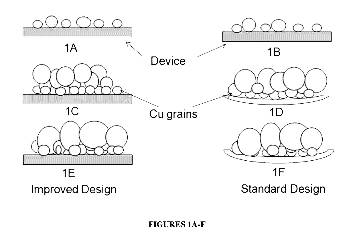
Even many of the improved copper electroplating baths directed to addressing the problems of internal stress have not been able to resolve the warping problem when plating on thin substrate.

Method used


Image

  • Method of electroplating low internal stress copper deposits on thin film substrates to inhibit warping
  • Method of electroplating low internal stress copper deposits on thin film substrates to inhibit warping
  • Method of electroplating low internal stress copper deposits on thin film substrates to inhibit warping

Examples


example 1

[0044]The following aqueous acid copper electroplating baths are prepared at room temperature.

TABLE 1ComponentBath 1Bath 2Copper sulfate160g / L160g / LSulfuric acid150g / L150g / LChloride (as hydrochloric acid)60ppm60ppmBis-sodium sulfopropyl disulfide4ppm03-mercapto-1-propane sulfonic6ppm0acid, sodium saltO-ethyldithiocarbonato)-S-0150ppm(3-sulfopropyl)-ester,potassium saltPolyoxy-alkylene glycol0.15g / L0.9g / LPolyethylene glycol0.18g / L1.1g / LBranched polyethylenimine0.75ppm0.75ppm(Mw = 25000)

[0045]The components of the copper electroplating baths are made up using conventional laboratory procedures where organics are added to water followed by adding the inorganic components. Stirring or agitation with heat application at temperatures of below 30° C. is done to be certain that all of the components are solubilized in the water. The baths are allowed to come to room temperature prior to copper electroplating. The pH of the acid copper electroplating baths ranges from less than 1 to 1 at roo...

example 2

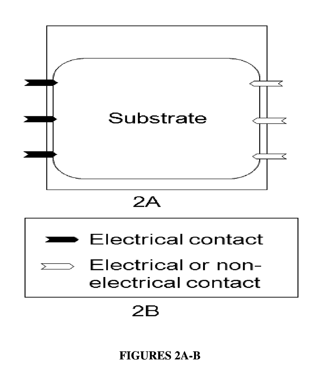
[0046]A plurality of thin films of copper having thicknesses of 100 μm are joined to non-conducting rectangular flat panel plating jigs as illustrated in FIG. 2A. Each thin film is secured to a flat panel plating jig by six electrical contacts, three on each side of the thin film or in the alternative by three electrical contacts and three non-electrical contacts as shown in FIGS. 2A and 2B. The non-conducting flat panel plating jigs with the thin films are secured to a conveyor system where the plating jig is joined to the conveyor such that it does not move outside a single plane and which transports the thin films through plating tanks which contain Bath 1 or Bath 2 as in Example 1. The thin films remain substantially in one plane during the electroplating process. When the thin copper films joined to the flat panel jigs pass into one of the two copper plating baths, the electrical contacts are placed under a potential from an electric rail which makes electrical contact with the...

example 3

[0047]The following aqueous acid copper electroplating baths are prepared at room temperature.

TABLE 2ComponentBath 3Copper sulfate160g / LSulfuric acid150g / LChloride (as hydrochloric acid)60ppm(O-ethyldithiocarbonato)-S-175ppm(3-sulfopropyl)-ester,potassium saltPolyoxy-alkylene glycol0.15g / L(PolyMax ™ PA-66 / LC solution)Polyethylene glycol0.18g / L(PEG 12000)Polyallylamine1.25ppm(Mw = 15000)

[0048]The components or the copper electroplating bath are made up using conventional laboratory procedures where organics are added to water followed by adding the inorganic components. Stirring or agitation with heat application at temperatures of below 30° C. is done to be certain that all of the components are solubilized in the water. The bath is allowed to come to room temperature prior to copper electroplating. The pH of the acid copper electroplating bath is less than 1 at room temperature and during copper electroplating.


PUM

PropertyMeasurementUnit
Thicknessaaaaaaaaaa
Stress optical coefficientaaaaaaaaaa
Ductilityaaaaaaaaaa

Abstract

Thin film substrates are electroplated with copper from low internal stress, high ductility acid copper electroplating baths. During the copper electroplating process the thin film substrates can warp or bow. To address the problem of warping or bowing during copper electroplating the thin film substrate is held by a securing means which inhibits the thin film substrate from excessive activity.

Description

FIELD OF THE INVENTION[0001]The present invention is directed to a method of electroplating low internal stress copper deposits on thin film substrates to inhibit warping of the thin film substrates. More specifically, the present invention is directed to a method of electroplating low internal stress copper deposits on thin film substrates to inhibit warping of the thin film substrates by using a securing means to inhibit excessive activity of the thin film substrate during copper electroplating.BACKGROUND OF THE INVENTION[0002]Internal or intrinsic stress of electrodeposited metals is a well known phenomenon caused by imperfections in the electroplated crystal structure. After the electroplating operation such imperfections seek to self correct and this induces a force on the deposit to contract (tensile strength) or expand (compressive stress). This stress and its relief can be problematic. For example, when electroplating is predominantly on one side of a substrate it can lead t...

Claims


Application Information

Patent Timeline
IPC IPC(8): C25D3/38C25D17/06C25D5/04
CPCC25D3/38C25D17/06C25D5/04C25D17/007C25D17/00C25D17/001H01L21/2885C25D7/123H01L21/67288
Inventor KAO, YU HUAWEI, LINGYUNGOMEZ, LUISLEFEBVRE, MARK
Owner ROHM & HAAS ELECTRONICS MATERIALS LLC
Learn More