Non-destructive acoustic metrology for void detection

a void detection and acoustic metrology technology, applied in the direction of semiconductor/solid-state device testing/measurement, semiconductor/solid-state device details, instruments, etc., can solve the problems of high aspect ratio vias with copper, one of the most difficult and expensive steps of the fabrication process, and the current methods are mostly destructiv

Active Publication Date: 2017-08-03
UNIV OF COLORADO THE REGENTS OF +1
View PDF3 Cites 7 Cited by
  • Summary
  • Abstract
  • Description
  • Claims
  • Application Information

AI Technical Summary

Problems solved by technology

Nevertheless, the process is complex and filling the high aspect ratio vias with copper is one of the most challenging and expensive steps of the fabrication process.
Current methods are mostly destructive and rely on off-line analysis at the feature of interest.
Cross-sectional focused ion beam (FIB) SEM is used extensively for the characterization of the voids and although it p

Method used


Image

  • Non-destructive acoustic metrology for void detection
  • Non-destructive acoustic metrology for void detection
  • Non-destructive acoustic metrology for void detection

Examples


Embodiment Construction

[0030]In the following detailed description, references are made to the accompanying drawings that form a part hereof, and in which are shown by way of illustrations specific embodiments or examples. These aspects may be combined, other aspects may be utilized, and structural changes may be made without departing from the spirit or scope of the present disclosure. The following detailed description is therefore not to be taken in a limiting sense, and the scope of the present disclosure is defined by the appended claims and their equivalents.

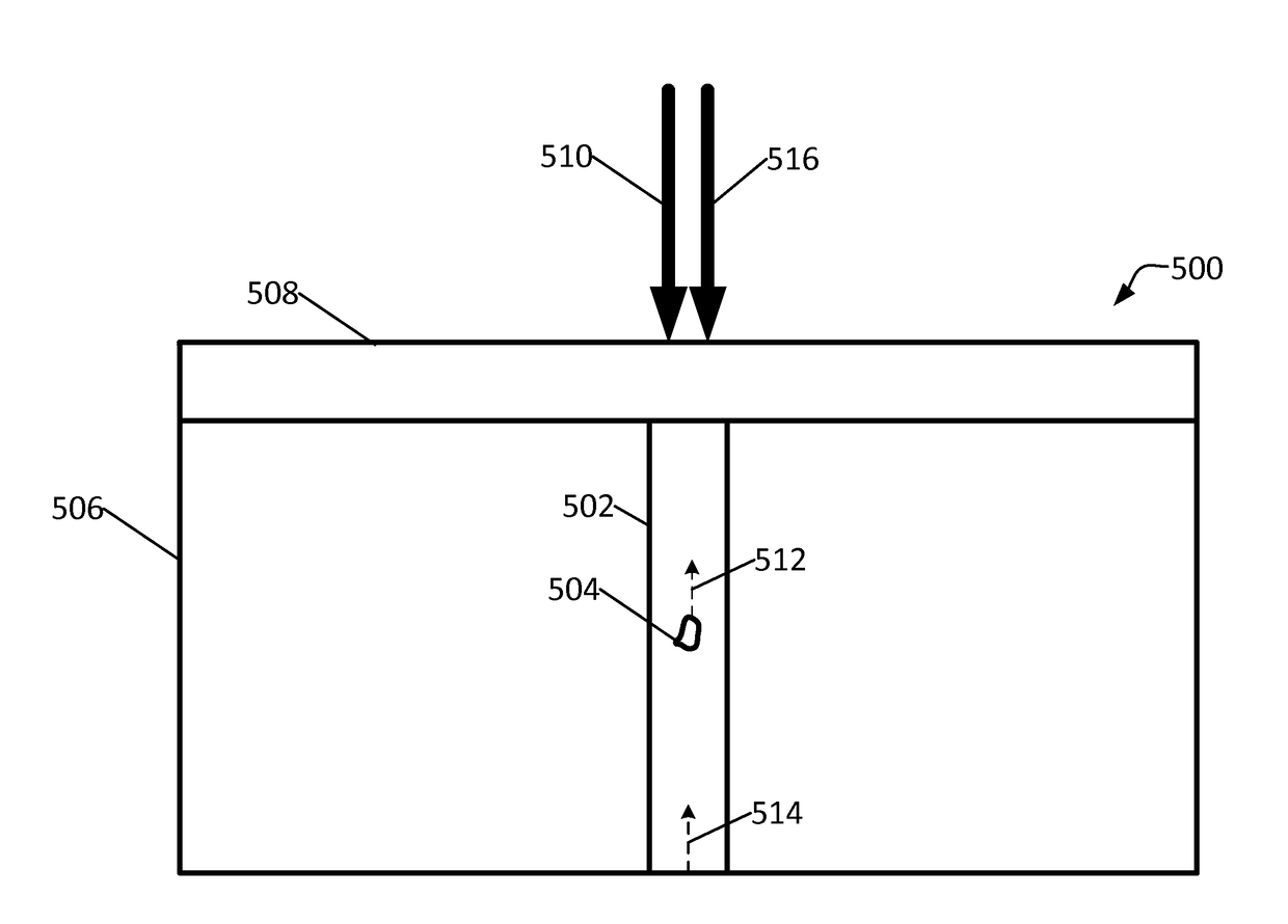
[0031]Laser based ultrasonics is a high sensitivity, non-contact technique for the nondestructive evaluation of materials with excellent temporal and spatial resolution. A pulsed laser source irradiates a specimen surface where some of the laser energy is absorbed, leading to local thermal expansion and elastic wave generation through the thermoelastic effect. The amplitude, frequency content, and directivity of the generated acoustic modes depe...


PUM


Abstract

Advanced interconnect technologies such as Through Silicon Vias (TSVs) have become an integral part of 3-D integration. Methods and systems and provided for laser-based acoustic techniques in which a short laser pulse generates broadband acoustic waves that propagate in the TSV structure. An optical interferometer detects the surface displacement caused by the acoustic waves reflecting within the structure as well as other acoustic waves traveling near the surface that has information about the structure dimensions and irregularities, such as voids. Features of voids, such as their location, are also identified based on the characteristics of the acoustic wave as it propagates through the via. Measurements typically take few seconds per site and can be easily adopted for in-line process monitoring.

Description

PRIORITY CLAIM[0001]This application is being filed on 29 Sep. 2015, as a PCT International Application, and claims the benefit of U.S. Provisional Application No. 62 / 056,773, filed on Sep. 29, 2014, the disclosure of which is incorporated herein by reference in its entirety.INTRODUCTION[0002]Microelectronics industry trends have continued to move rapidly towards 3-D integration of semiconductor devices and the driving force remains the need for smaller, faster devices with optimized performance, enhanced data transfer speeds, minimum transmission loss, while maintaining reliability and meeting cost targets. Through-silicon via (TSV) technology has entered the mainstream for 3D ICs as they support heterogeneous integration of logic and memory devices resulting in significant improvements in performance. Depending on the application, a “Via-first” or “Via-last” approach may be used in manufacturing. Nevertheless, the process is complex and filling the high aspect ratio vias with copp...

Claims


Application Information

Patent Timeline
IPC IPC(8): H01L21/66G01N29/46G01N29/24H01L21/768G01N29/04
CPCH01L22/12H01L21/76898G01N2291/0289G01N29/2418G01N29/46G01N29/04G01N29/06G01N29/0681G01N29/069G01N29/07H01L22/20
Inventor MEHENDALE, MANJUSHAKOTELYANSKII, MICHAELMURRAY, TODD W.MAIR, ROBINMUKUNDHAN, PRIYADOVE, JACOB D.RU, XUEPINGCOHEN, JONATHANKRYMAN, TIMOTHY
Owner UNIV OF COLORADO THE REGENTS OF
Why Eureka
Try Eureka