Metal halide perovskite light emitting device and method of manufacturing the same

a technology of light-emitting devices and metal halide perovskite, which is applied in the direction of solid-state devices, semiconductor devices, thermoelectric devices, etc., can solve the problems of difficult adjustment of the size of quantum dots during the synthesis process, color purity may be deteriorated, and the limitation of manufacturing low-priced products of organic light-emitting diodes and inorganic quantum dots, so as to prevent the dissociation of excitons

Inactive Publication Date: 2017-08-03
POSTECH ACAD IND FOUND
View PDF1 Cites 33 Cited by
  • Summary
  • Abstract
  • Description
  • Claims
  • Application Information

AI Technical Summary

Benefits of technology

[0022]Example embodiments of the present invention provide a metal halide perovskite light emitting device capable of preventing dissociation of excitons at the interface between a metal halide perovskite light emitting layer and electrodes and coming in ohmic contact with the metal halide perovskite light emitting layer, and a method of manufacturing the same.

Problems solved by technology

However, the organic light emitting diodes have high efficiency, but have a drawback in that the color purity may be deteriorated due to a wide full width at half maximum of an emission spectrum, and the inorganic quantum dots in which color is adjusted according to the size of the quantum dots have high color purity, but have a drawback in that it is very difficult to adjust the size of the quantum dot during a synthesis process.
Also, the organic light emitting diodes and the inorganic quantum dot materials have a limitation in manufacturing low-priced products due to high manufacturing costs.
As a result, since the organic ammonium does not emit light of high color purity (a full width at half maximum of less than 30 nm), the full width at half maximum of an emission spectrum should become wider than 50 nm, which makes the organic ammonium unsuitable for light emitting layers.
Therefore, in this case, the organic ammonium is very unsuitable for phosphors having high color purity (a full width at half maximum of less than 30 nm) emphasized in this patent application.
Although such a metal halide perovskite has advantages as the light emitting diode, the metal halide perovskite has a problem of limited application to light emitting diodes.
First, a problem such as a decline in efficiency of a light emitting diode is caused due to various types of defects present inside perovskites.
That is, since such defects exist out of an energy level of a conduction band or a valence band, the electrons or holes are trapped at an energy level of the defects to limit movement of charges and induce unwanted non-radiative recombination.
In the light emitting diodes in which the balance between the electrons and the holes is important, the perovskites having the p-type characteristics have a problem in that they have no option but to exhibit low efficiency.
In this way, the metal halide perovskite thin film has a drawback in that it is difficult to implement using a thin film manufacturing process (in which a device having higher efficiency has a higher grain size (>200 nm) and a severe surface unevenness) used in metal halide solar cells known in the art.
Fifth, since transparent metal oxide electrodes of a metal halide perovskite light emitting device have a property of being easily broken due to instability when the transparent metal oxide electrodes are bent, they are difficult to apply to flexible metal halide perovskite light emitting devices.

Method used


Image

  • Metal halide perovskite light emitting device and method of manufacturing the same
  • Metal halide perovskite light emitting device and method of manufacturing the same
  • Metal halide perovskite light emitting device and method of manufacturing the same

Examples


example 1

Preparative Manufacture of Conductive Layer

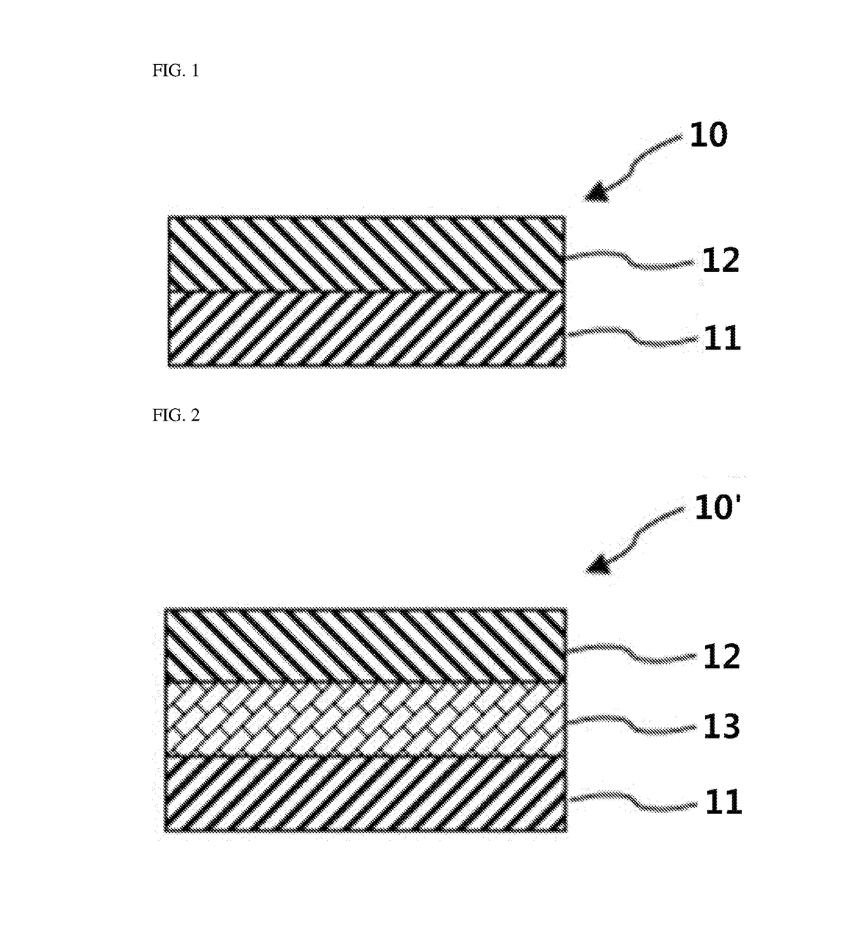
[0200]For a conductive layer, a mixture including a highly conductive poly(3,4-ethylenedioxythiophene):poly(styrenesulfonate) (PEDOT:PSS) solution (PH500 commercially available from H.C. Starck GmbH: having a PSS content of 2.5 parts by weight per 1 part by weight of PEDOT and a conductivity of 0.3 S / cm), a solution of the following polymer 100 (5% by weight of polymer 100 was dispersed in a mixture of water and an alcohol (water:alcohol=4.5:5.5 (v / v)); commercially available from Aldrich Co. Ltd.), and 5% by weight of dimethyl sulfoxide (DMSO) was prepared. Here, a mixing ratio of the PEDOT:PSS solution and the solution of polymer 100 was adjusted so that the content (based on solid contents) of polymer 100 per 1 part by weight of PEDOT was 1.0 parts by weight

[0201](In polymer 100, x=1,300, y=200, and z=1)

[0202]The mixture was spin-coated onto a glass substrate, and then heat-treated at 200° C. for 10 minutes to form a conductive layer 1 ...

example 2

Preparative Manufacture of First Electrode (Anode)

[0208]A solution obtained by diluting the solution of polymer 100 with isopropyl alcohol (1:10, v / v) was spin-coated onto the conductive layer 4 described in Preparative Example 1 at 4,500 rpm for 90 seconds, and then heat-treated at 150° C. for 201 nanoseconds to form a surface energy-tuning layer on the conductive layer 4, thereby manufacturing a first electrode.

example 3

Preparative Manufacture of Metal Halide Perovskite Light Emitting Device

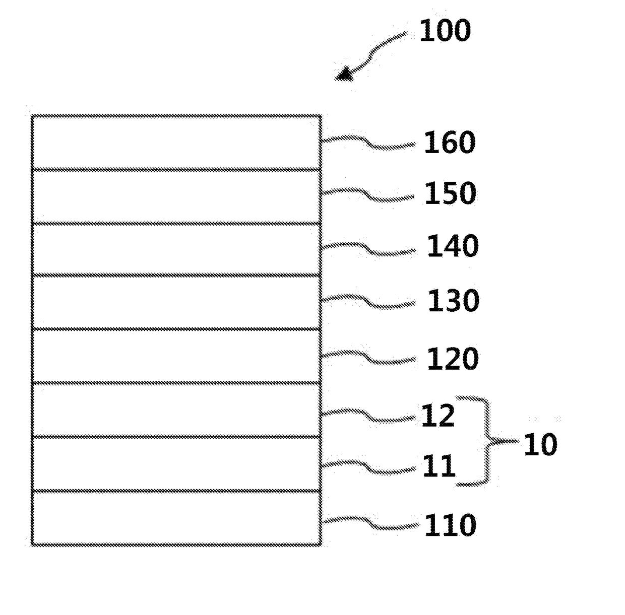
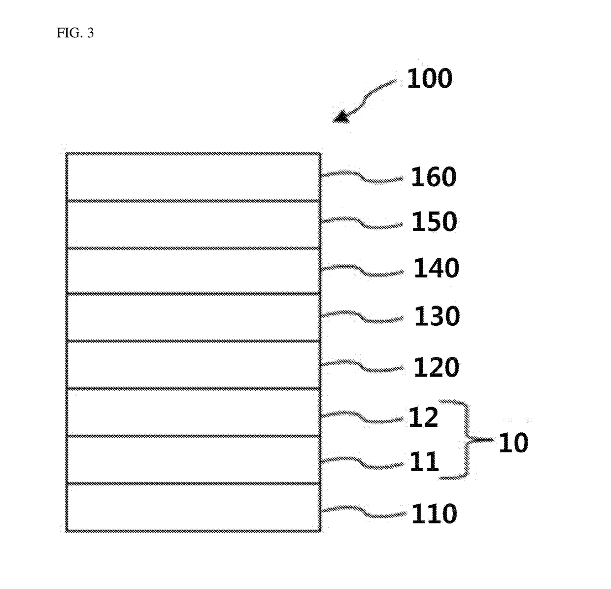
[0209]As an anode, a first electrode was formed on a glass substrate according to the method described in Preparative Example 2, and then CH3NH3Br and PbBr2 were mixed at a ratio of 1.05:1, and 40% by weight of the resulting mixture was dissolved in dimethyl sulfoxide (DMSO). Thereafter, a CH3NH3PbBr3 solution was spin-coated to form a CH3NH3PbBr3 light emitting layer having a thickness of 300 nm.

[0210]A 50 nm-thick TPBi electron transport layer, a 1 nm-thick LiF electron injection layer, and a 100 nm-thick Al cathode (a second electrode) were sequentially formed on the CH3NH3PbBr3 light emitting layer (this was performed using a vacuum deposition method) to manufacture a metal halide perovskite light emitting device 1


PUM

PropertyMeasurementUnit
full width at half maximumaaaaaaaaaa
exciton diffusion lengthaaaaaaaaaa

Abstract

Provided are a metal halide perovskite light emitting device and a method of manufacturing the same. The metal halide perovskite light emitting device includes a substrate, a first electrode formed on the substrate, a light emitting layer formed on the first electrode and including a metal halide perovskite material, and a second electrode disposed on the light emitting layer, the first electrode includes a conductive layer and a surface energy-tuning layer disposed on the conductive layer, the conductive layer includes a conductive polymer and a first fluorine-based material, and the surface energy-tuning layer includes a second fluorine-based material but does not include the conductive polymer. Therefore, the first electrode can come in ohmic contact with a metal halide perovskite light emitting layer by adjusting a work function, and can prevent the dissociation of excitons to enhance luminous efficiency, thereby effectively improving efficiency of a light emitting device.

Description

CLAIM FOR PRIORITY[0001]This application claims priority to Korean Patent Application No. 10-2016-0010807 filed on Jan. 28, 2016 in the Korean Intellectual Property Office (KIPO), the entire contents of which are hereby incorporated by reference.BACKGROUND[0002]1. Technical Field[0003]Example embodiments of the present invention relate in general to a metal halide perovskite light emitting device and a method of manufacturing the same, and more particularly, to a metal halide perovskite light emitting device having improved luminous efficiency, and a method of manufacturing the same.[0004]2. Related Art[0005]In recent years, the display industry has been changed from inorganic light emitting diodes (LEDs) to organic light emitting diodes. The organic light emitting diodes have characteristics such as a relatively simple and lightweight structure and processability as well as a flexible characteristic, and thus have come into the spotlight as next-generation flexible electronic devic...

Claims


Application Information

Patent Timeline
Patent Type & Authority Applications(United States)
IPC IPC(8): H01L51/00
CPCH01L51/0077H01L51/0037H01L51/0035H01L51/0034H01L51/0021H01L51/56H01L51/5206H01L51/5221H01L51/5012H10K71/60H10K85/1135H10K85/60H10K50/81H10K85/30H10K85/10H10K85/111H10K50/11H10K50/82H10K71/00
Inventor LEE, TAE-WOOJEONG, SU-HUN
Owner POSTECH ACAD IND FOUND
Why Eureka
Try Eureka