
Package substrate differential impedance optimization for 25 to 60 gbps and beyond

a technology of differential impedance optimization and substrate, applied in multi-objective optimisation, cad techniques, instruments, etc., can solve the problems of reduced signal quality, increased differential return loss, reduced eye height and eye width

Active Publication Date: 2017-08-10
SARCINA TECH LLC
View PDF1 Cites 18 Cited by
  • Summary
  • Abstract
  • Description
  • Claims
  • Application Information

AI Technical Summary

Benefits of technology

The patent provides special designs for BGA ball assignment, via and PTH placement, metal void and shielding balance, and trace width adjustment near the transition location. These designs can meet high volume manufacturing design rules and pass rigorous quality and reliability tests. In summary, the patent provides technical means to address challenges in the design process for BGA balls.

Problems solved by technology

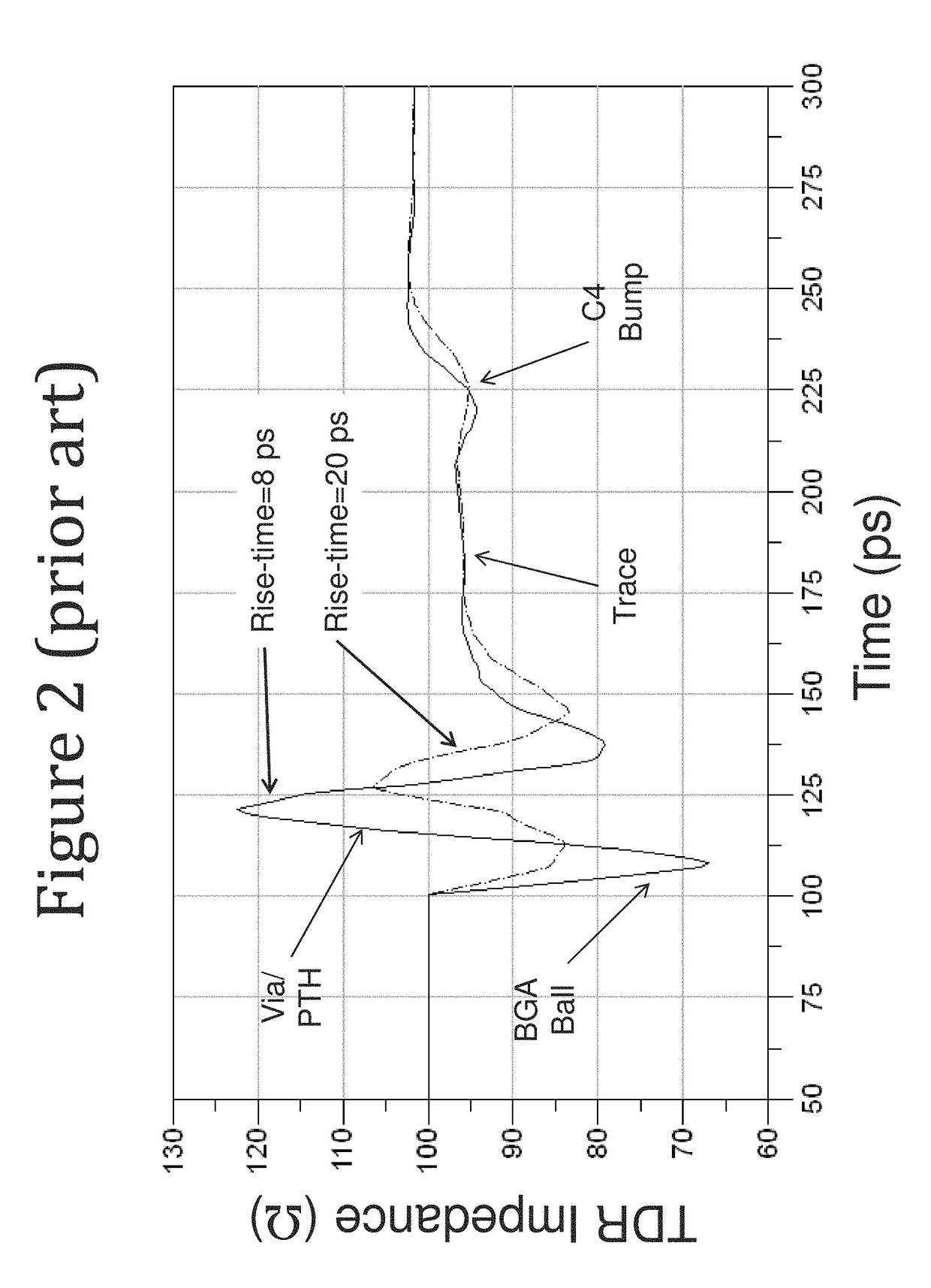
A high package impedance discontinuity from ball grid array (B GA) ball to C4 bump will lead to large signal reflections, increased differential return loss, and degraded signal quality and as a result, reduced eye height and eye width.
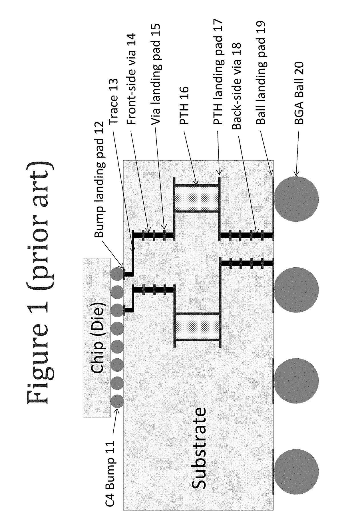
Unfortunately, in a semiconductor package the impedance mismatch is considered natural because of different substrate structures: BGA ball, via, PTH (plated-through-hole), trace, and C4 bump.
Having them Connected together naturally brings impedance mismatch.
The dramatic increase in substrate impedance discontinuity at 25 Gb / s and beyond has made it hard to meet minimum differential return loss specifications from various organizations and has become a major issue in SerDes signal transmission.
Nevertheless, at 25 Gb / s data rate and beyond, these simple approaches are no longer effective in achieving the desired values of less than ±10% differential impedance variation from BGA ball to C4 bump.
Notwithstanding, for a vertical interconnection, maintaining a 100-Ohm differential impedance from BGA ball to C4 bump (including vias and PTHs) is challenging because the diameters, heights and spacing of these structures are vastly different from each other.
In other words, the impedance mismatch increases with the increase of data rate.
Because of the high impedance discontinuity and the large signal reflection as well as the big differences in structure, vertical differential impedance optimization to lower its variation becomes challenging.
However, the various landing pads from layer to layer make the impedance even worse and more difficult to manage.
Finally, the transition from vertical interconnection to horizontal interconnection imposes a challenge to package designer because matching the impedance at the transition point is difficult.

Method used


Image

  • Package substrate differential impedance optimization for 25 to 60 gbps and beyond
  • Package substrate differential impedance optimization for 25 to 60 gbps and beyond
  • Package substrate differential impedance optimization for 25 to 60 gbps and beyond

Examples


first embodiment

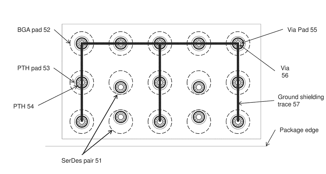
[0075]FIG. 4b shows the design of the BGA ball and the bottom metal layer of the first embodiment of this invention. FIG. 4a shows the BGA ball and the bottom metal layer of a conventional 10 Gb / s design. In FIGS. 4a and 4b, the letter “G” indicates ground balls under the anti-pad. As shown in FIG. 4a, in the conventional design a SerDes differential pair is surrounded with fully populated ground BGA balls. The metal ground plane 41 covers all the SerDes areas and has all the ground BGA balls connected except in the antipad region 42. It relies on enlarging the antipad 42 size to optimize impedance by reducing the parasitic capacitance between the BGA ball and the ground plane. The shielding is not in the signal vertical propagation direction and their contribution to crosstalk reduction between adjacent SerDes signals is minimal. On the other hand, it dramatically reduces the impedance because of the large capacitive coupling between it and the SerDes signals.

[0076]The first embodi...

second embodiment

[0086]FIGS. 10a-10d illustrate the SerDes differential pair design according to a second embodiment of the present invention. To make the drawing easy to view, only the SerDes pair is shown; all its surrounding BGA landing pads, vias, PTHs, voids, and shielding are removed. FIG. 10a is a top view. FIG. 10b is a perspective view. FIG. 10c is a side view in a direction from the lower side of FIG. 10a and FIG. 10d is a side view in a direction from the right side of FIG. 10a.

[0087]As shown in FIG. 10a, a key difference between this design of the second embodiment and the design of the first embodiment is the “90 degree rotation” of the vertical plane that passes through the PTH 101 pair (and all the vias 102 above them on the upper side of the PTH) relative to the vertical plane that passes through the corresponding BGA ball pads 103. Also, the PTH 101 pair and the vias 102 above them are located at the center plane between the two BGA ball pads 103 and are kept equal distance to each...

third embodiment

[0116]The third embodiment is a novel design in BGA ball assignment, via and PTH placement, metal void and shielding balance, and trace width adjustment near the transition location are provided. Different from the first and second embodiments which used stripline structure for horizontal interconnection, the third embodiment uses microstrip line structure routed on top and bottom metal layers for horizontal interconnection. The advantage of microstrip line over stripline is that package substrate layout count can be reduced and the packaging cost can be lowered. It should be noted that the design of the third embodiment uses standard package substrate design rules and can be manufactured in high volume without the increase in cost, and can pass rigorous quality and reliability tests.

[0117]Compared to the relatively expensive ceramic package, today, the HFCBGA (Heat spreader Flip-Chip Ball-Grid-Array) package with organic substrate is still the preferred package type for 25 Gb / s Ser...


PUM


Abstract

Package design method for semiconductor chip package for high speed SerDes signals for optimization of package differential impedance and reduction of package differential insertion loss and differential return loss at data rates of 25 to 60 Gb / s and beyond. The method optimizes parameters of vertical interconnections of BGA ball, via, and PTH, and around the joint between vertical and horizontal interconnections of traces. Also disclosed are examples of chip package designs for high speed SerDes signals, including one using 0.8 mm BGA ball pitch and 10-layer buildup substrate, one using 1 mm BGA ball pitch and 14-layer buildup substrate, one using 6-layer buildup substrate with signals routed on top and bottom metal layers with microstrip line structure, and one using 12-layer package substrate with unique via configuration, all of which achieve low substrate differential impedance discontinuity, reduced differential insertion loss and differential return loss between BGA balls and C4 bumps.

Description

BACKGROUND OF THE INVENTION[0001]Field of the Invention[0002]This invention relates to semiconductor chip package design for high speed SerDes signals which achieves low insertion loss, low return loss, and low substrate differential impedance discontinuity between BGA balls and C4 bumps. It also provides an optimization method for calculating parameters of such a package.[0003]Description of the Related Art and Background[0004]To meet the ever increased challenge for high speed chip-to-chip communication, today's semiconductor chips often use high speed SerDes (Serializer / Deserializer) interconnection technology. The cutting edge SerDes data rate has increased from 10 Gb / s to 25-28 Gb / s. SerDes differential impedance discontinuity of a flip-chip package is a key gauge in determining SerDes eye diagram quality. A high package impedance discontinuity from ball grid array (B GA) ball to C4 bump will lead to large signal reflections, increased differential return loss, and degraded sig...

Claims


Application Information

Patent Timeline
IPC IPC(8): H01L23/66H04B1/40G06F17/50H01L23/498H01L23/00
CPCH01L23/66H01L23/49822H01L23/49827H01L23/49838H01L24/16G06F2217/40H04B1/40H01L2224/16227H01L2223/6616H01L2223/6638G06F2217/08G06F17/5009H01L23/49816H01L23/50H01L2223/6655H01L2924/15311H01L2924/3011H01L2924/3025G06F30/367G06F30/39G06F30/20G06F2111/06G06F2113/18G06F2115/12
Inventor ZU, LONGQIANGHSIAO, LI-CHANG
Owner SARCINA TECH LLC
Learn More