
Eureka
For R&D, Eureka makes reading and utilizing patents & technical documents easy.
Eureka AIR
Designed for self-driven R&D workflows. Generate viable solutions, solve complex R&D challenges, empower your innovation with AI.

Eureka Materials
Designed for material experts only. Revolutionize your material R&D, from search, analyze, to developing new materials.

TechResearch
Generate reliable direction feasibility study reports for your R&D in just a few steps.

TechSeek
Discover and master advanced knowledge NOW. Basics, ideas, possibilities, all at once.

TechMind
As an expert in R&D Theories, TechMind can generates customized viable solutions instantly.

TechRisk
Analyze your overall solution with one click, know your potential R&D risks in advance.

TechMonitor
Get weekly tech updates, stay abreast of the latest tech innovations and key insights.
Red organic electroluminescent device and preparation method thereof
- Summary
- Abstract
- Description
- Claims
- Application Information
AI Technical Summary
Benefits of technology
Problems solved by technology
Method used
Image

Examples
example 1
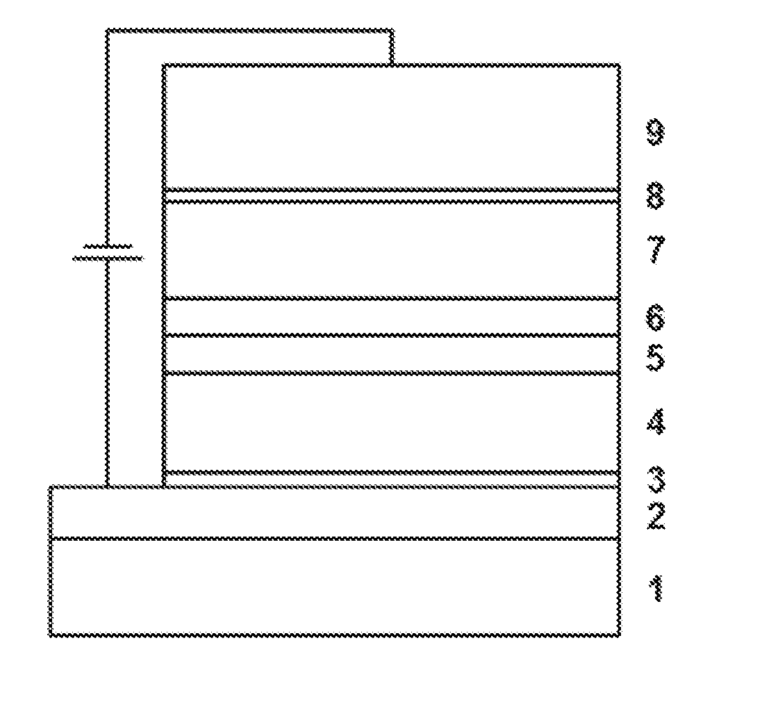
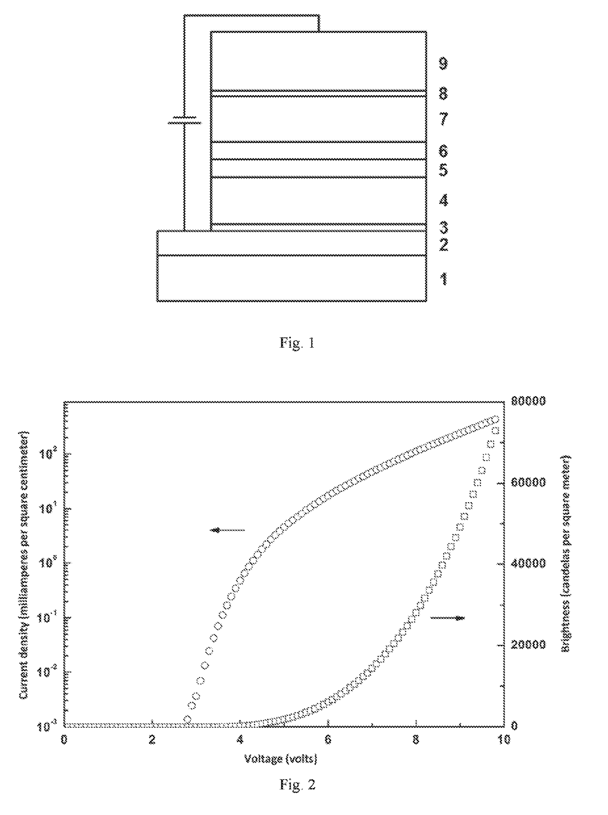
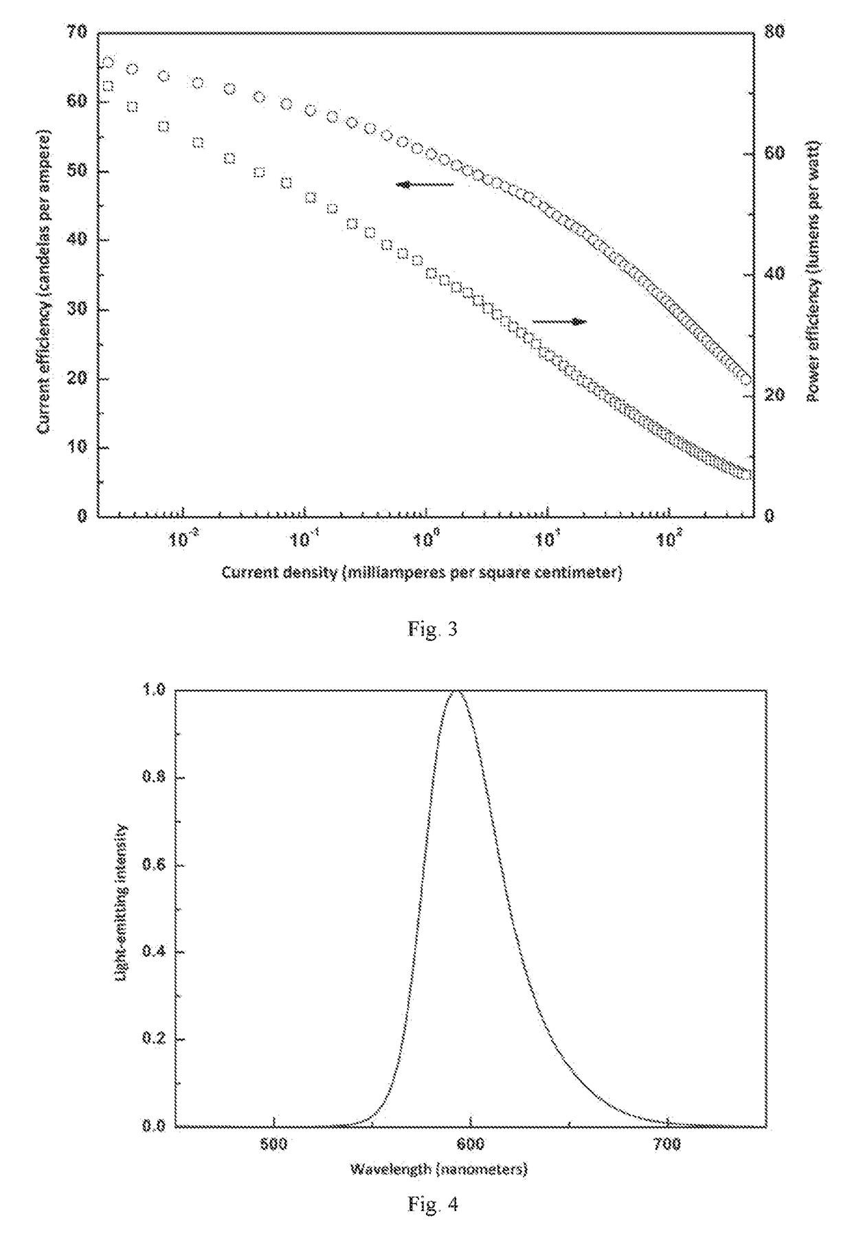
[0084]An ITO anode layer on an ITO glass was laser-etched into a strip electrode, then ultrasonically cleaned sequentially with a cleaning liquid and deionized water for 15 min, and placed in an oven for drying. The dried substrate was then placed in a pretreated vacuum chamber, and the ITO anode was subjected to a low-pressure plasma treatment for 3 min under an atmosphere having a vacuum degree of 10 Pa with a voltage of 400V and then transferred to an organic evaporation plating chamber. In an organic evaporation plating chamber with a vacuum degree of 1-2×10⁻⁵ Pa, a MoO3 anode modification layer 3 having a thickness of 3 nm, a TAPC hole transporting-electron blocking layer 4 having a thickness of 40 nm, a TcTa hole-dominated light-emitting layer 5 doped with PQ2Ir(dpm) having a thickness of 10 nm, a CzSi electron-dominated light-emitting layer 6 co-doped with Tb(acac)3phen and PQ2Ir(dpm) having a thickness of 10 nm, and a TmPyPB hole blocking-electron transporting layer 7 having...
example 2
[0088]An ITO anode layer on an ITO glass was laser-etched into a strip electrode, then ultrasonically cleaned sequentially with a cleaning liquid and deionized water for 15 min. and placed in an oven for drying. The dried substrate was then placed in a pretreated vacuum chamber, and the ITO anode was subjected to a low-pressure plasma treatment for 3 min under an atmosphere having a vacuum degree of 10 Pa with a voltage of 400V and then transferred to an organic evaporation plating chamber. In an organic evaporation plating chamber with a vacuum degree of 1-2×10⁻⁵ IPa, a MoO3 anode modification layer 3 having a thickness of 3 nm, a TAPC hole transporting-electron blocking layer 4 having a thickness of 40 nm, a mCP hole-dominated light-emitting layer doped with PQ2Ir(dpm) 5 having a thickness of 10 nm, a 26DCzPPy electron-dominated light-emitting layer 6 co-doped with Eu(TTA)3phen and PQ2Ir(dpm) having a thickness of 10 nm, and a TmPyPB hole blocking-electron transporting layer 7 hav...
example 3
[0090]An ITO anode layer on an ITO glass was laser-etched into a strip electrode, then ultrasonically cleaned sequentially with a cleaning liquid and deionized water for 15 min, and placed in an oven for drying. The dried substrate was then placed in a pretreated vacuum chamber, and the ITO anode was subjected to a low-pressure plasma treatment for 3 min under an atmosphere having a vacuum degree of 10 Pa with a voltage of 400V and then transferred to an organic evaporation plating chamber. In an organic evaporation plating chamber with a vacuum degree of 1-2×10⁻⁵ Pa, a MoO3 anode modification layer 3 having a thickness of 3 nm, a TAPC hole transporting-electron blocking layer 4 having a thickness of 40 nm, a TcTa hole-dominated light-emitting layer 5 doped with PQ2Ir(dpm) having a thickness of 10 nm, a 26DCzPPy electron-dominated light-emitting layer 6 co-doped with Eu(DBM)3phen and PQ2Ir(dpm) having a thickness of 10 nm, and a TmPyPB hole blocking-electron transporting layer 7 hav...
PUM
 Abstract
Description
Claims
Application Information
 - R&D Engineer
- R&D Manager
- IP Professional
- Industry Leading Data Capabilities
- Powerful AI technology
- Patent DNA Extraction
Browse by: Latest US Patents, China's latest patents, Technical Efficacy Thesaurus, Application Domain, Technology Topic, Popular Technical Reports.
© 2024 PatSnap. All rights reserved.Legal|Privacy policy|Modern Slavery Act Transparency Statement|Sitemap|About US| Contact US: help@patsnap.com