Display driver backplane, display device and fabrication method

a technology of display device and backplane, which is applied in the field of display technology, can solve the problems of increasing size, complex or even infeasible processing, and increasing the cost of the fabrication process, and achieves the effects of reducing cost, improving device performance, and low processing cos

Inactive Publication Date: 2017-12-14
SHANGHAI JUEXIN PHOTOELECTRIC TECH CO LTD
View PDF6 Cites 18 Cited by
  • Summary
  • Abstract
  • Description
  • Claims
  • Application Information

AI Technical Summary

Benefits of technology

[0020]Compared to the prior art, the display driver backplane of the present invention employs a technique in which two or three chips are stacked together, enabling placement of transistors with various capabilities in different layers, which are interconnected using a deep via technique, with electrodes disposed on the top layer driving and controlling the display panel. This addresses the prior-art issues of high difficulty in fabricating transistors with different capabilities in the same layer and costly interconnection between transistors in different chips, resulting in significant improvements in device performance and reductions in cost.
[0021]Therefore, in principle, the deficiencies of the aforesaid system-on-chip architecture may be resolved by a solution in which multiple chips are stacked together three-dimensionally, with sub-circuits of different MOS transistors fabricated by different processes being interconnected into a system using the via technology. The present invention just discloses such a solution in which multiple chips are three-dimensionally stacked to foul′ a micro display backplane driver system at low processing cost and high integration.

Problems solved by technology

As a result, forming a system-on-chip architecture for the backplane driver system constructed from multiple sub-circuits composed of various MOS transistors on a single semiconductor substrate, particularly on the same silicon substrate, will not only impose a great challenge on but will also lead to great increases in the cost of the fabrication process, making the process complex or even infeasible.
Additionally, integrating circuits of different functions on the same semiconductor substrate will also lead to an increase size and reduced performance, particularly a lower operational speed and higher power consumption, of a chip integrating such a micro display backplane driver system.

Method used


Image

  • Display driver backplane, display device and fabrication method
  • Display driver backplane, display device and fabrication method
  • Display driver backplane, display device and fabrication method

Examples


first embodiment

[0029 of Display Driver Backplane

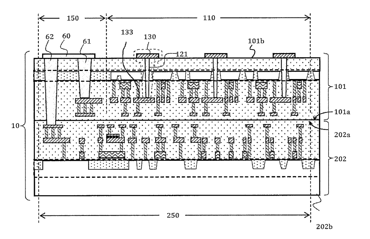
[0030]Referring to FIG. 1, a display driver backplane 10 according to this embodiment includes: a first semiconductor laminate 101 having a first surface 101a and a second surface 101b opposing the first surface, wherein a first semiconductor chip in the first semiconductor laminate 101 includes a pixel-driver array 110 consisting of a plurality of pixel driver elements and a first peripheral circuit unit 150; a first-electrode array 130 on the second surface 101b of the first semiconductor laminate; a second semiconductor laminate 202 having a first surface 202a and a second surface 202b opposing the first surface, wherein a second semiconductor chip in the second semiconductor laminate 202 includes a second peripheral circuit unit 250, and the first surface 202a of the second semiconductor laminate is boned to the first surface 101a of the first semiconductor laminate; and first vias 121 which are formed within the first semiconductor laminate 101 ...

second embodiment

[0036 of Display Driver Backplane

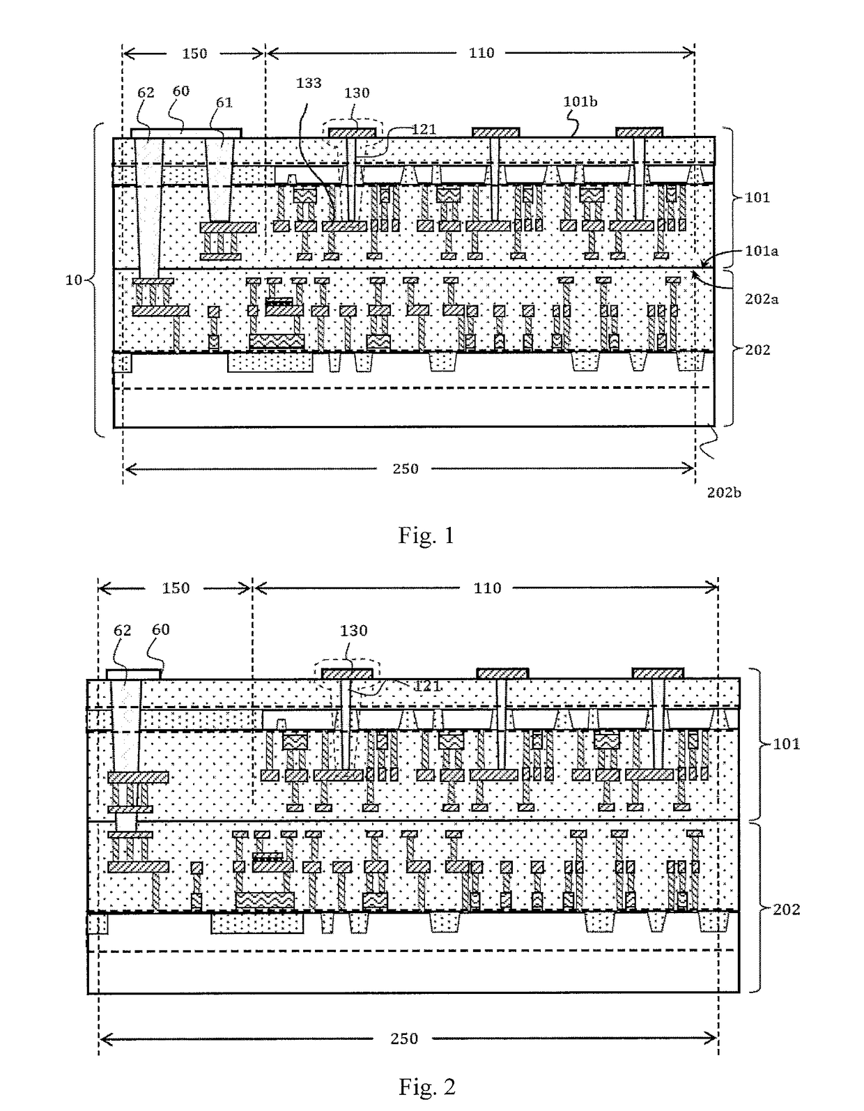
[0037]Referring to FIG. 2, a description of features in this embodiment that are the same as those in the first embodiment is omitted here for the sake of simplicity and clarity. This embodiment differs from the first embodiment in that, in lieu of the second and third vias, a fourth via 63 is included which penetrates through first semiconductor laminate 101 and terminates within the second semiconductor laminate 202, vertically electrically interconnecting the first peripheral circuit unit 110 and the second peripheral circuit unit 250.

[0038]In this embodiment, the fourth via 63 vertically connecting the first peripheral circuit in the first semiconductor laminate and the second peripheral circuit in the second semiconductor laminate allows a simpler configuration of the circuits.

third embodiment

[0039 of Display Driver Backplane

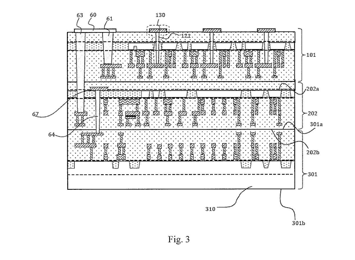
[0040]Referring to FIG. 3, a description of features in this embodiment that are the same as those in the first embodiment is omitted here for the sake of simplicity and clarity. This embodiment differs from the first embodiment in further comprising a third semiconductor laminate 301 bonded to the second surface 202b of the second semiconductor laminate. The third semiconductor laminate 301 comprises a first surface 301a and a second surface 301b opposing the first surface. The third semiconductor laminate is bonded to the second surface 202b of the second semiconductor laminate at the first surface 301a. The third semiconductor laminate 301 includes a third chip containing a third peripheral circuit unit 310. In this embodiment, the third peripheral circuit is a memory cell array.

[0041]In this embodiment, the bonding is performed in a different manner due to the additionally stacked chip. As the second semiconductor laminate and the third semicondu...


PUM


Abstract

A display driver backplane, a display device and a fabrication method thereof are disclosed. The display driver backplane includes: a first semiconductor laminate including pixel driver array consisting of a plurality of pixel driver elements and first peripheral circuit unit; first electrode array formed on second surface of first semiconductor laminate; a second semiconductor laminate containing a second peripheral circuit unit, wherein a first surface of the second semiconductor laminate is bonded to a first surface of first semiconductor laminate; and first vias that are formed within first semiconductor laminate and electrically interconnect first-electrode array and pixel-driver array. The present invention addresses prior-art issues of high difficulty in fabricating transistors with different capabilities in the same layer and costly interconnection between transistors in different chips by employing a technique in which two or three chips are stacked together, and hence achieves significant improvements in device performance and reductions in cost.

Description

CROSS-REFERENCES TO RELATED APPLICATIONS[0001]This application claims the priority of Chinese patent application number 201610420503.3, filed on Jun. 13, 2016, the entire contents of which are incorporated herein by reference.TECHNICAL FIELD[0002]The present invention relates to the field of display technology and, in particular, to a display driver backplane with a stack of multiple chips, a display device and a fabrication method.BACKGROUND[0003]A micro display backplane is an active matrix display device integrating an active matrix of light-emitting diodes or spatial light modulation (SLM) pixel elements to an array corresponding to a pixel driver circuit and a peripheral circuit on a single substrate. Common light-emitting diodes and spatial light modulation pixel elements include LED, OLED, liquid crystal display (LCD) and MEMS optical modulators. MEMS optical modulators include digital micro-mirror devices and digital micro shutters. The pixel driver circuit and peripheral ci...

Claims


Application Information

Patent Timeline
Patent Type & Authority Applications(United States)
IPC IPC(8): G09G3/36G09G3/34
CPCG09G3/3655G09G3/3406G09G3/3688G09G3/3677H01L23/481H01L25/0657H01L25/50H01L21/561H01L24/00H01L25/0753H01L33/62H10K59/131
Inventor WANG, XIAOCHUAN
Owner SHANGHAI JUEXIN PHOTOELECTRIC TECH CO LTD
Why Eureka
Try Eureka