Process of forming a photoactive layer of an optoelectronic device

Active Publication Date: 2018-01-04
COMMONWEALTH SCI & IND RES ORG
View PDF3 Cites 8 Cited by
  • Summary
  • Abstract
  • Description
  • Claims
  • Application Information

AI Technical Summary

Benefits of technology

[0174]Advantageously, each of the deposition method includes a manner of monitoring the quality of the metal M being deposited. In this way, the uniformity and other quality par

Problems solved by technology

Large scale production of these types of PV cells is difficult because the process of applying the photoactive layer has been found to be difficult to scale.
Whilst the resulting films exhibit satisfactory perovskite film coverage and uniformity, this technique demands high vacuum, and therefore is very energy intensive in a scaled up process.
However, it is not possible to use spin coating on a larger scale.
In wet coating, the wet film is susceptible to dewetting, non-homogenous crystal for

Method used


Image

  • Process of forming a photoactive layer of an optoelectronic device
  • Process of forming a photoactive layer of an optoelectronic device
  • Process of forming a photoactive layer of an optoelectronic device

Examples


example 1

Electrochemical Deposition of Pb Thin Film Seed Layer for Planar Perovskite Solar Cells

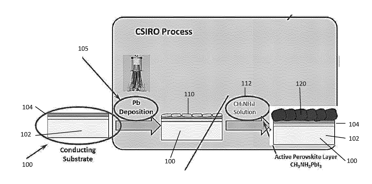
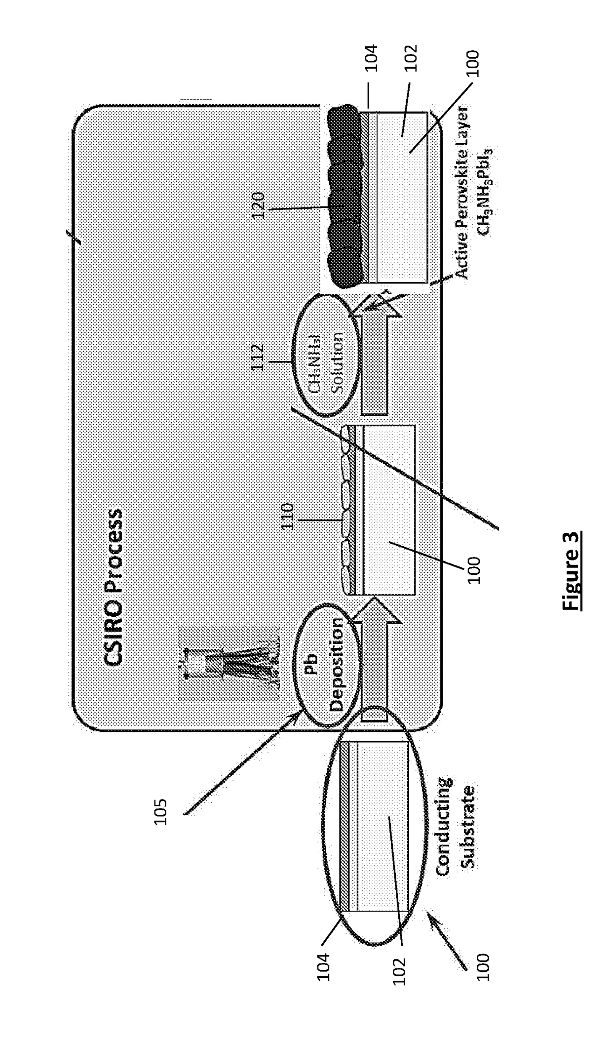
[0263]In this example, a thin metallic Pb seed layer is electrochemically deposited on an n-type compact blocking layer, in this case TiO2, as a precursor for a perovskite solar cell. The deposited Pb seed layer is then chemically converted to the photoactive perovskite material.

[0264]It should be appreciated that whist demonstrated for planar perovskite solar cells, the method and techniques exemplified can equally be applied to non-planar perovskite solar cells configurations for example the inclusion of a mesoscopic thin-film of nanoparticles for example TiO2, Al2O3, ZrO2 or the like.

1.1 Electrochemical Deposition of Pb

[0265]The electrochemical deposition equipment included the following:

[0266]An electrolyte consisting of a 0.01 mol / L solution of Pb(NO3)2 as Pb source and 0.1 mol / L KNO3 as inert conducting electrolyte (also known as supporting electrolyte.

[0267]A working electrode (that where t...

example 2

Thermal Evaporation of Thin Pb Film as Perovskite Seed Layer for Planar Perovskite Solar Cells

[0275]In the following two examples (2.1 and 2.2), a thin metallic Pb seed layer is formed by thermal evaporation of Pb and condensation onto an n-type compact blocking layer (in this example either ZnO or TiO2) as a precursor for a perovskite solar cell. The seed layer once deposited is then chemically converted to the photoactive perovskite material.

2.1 ZnO Blocking Layer on Indium-Doped Tin Oxide (ITO) Substrate Embodiment

2.1.1 Substrate Preparation

[0276]The ITO substrate was cleaned by successive sonication treatments in detergent (Hellmanex, 1% in milli-W water), pure milli-Q water and isopropanol.

[0277]ZnO blocking layer was applied by spin casting a suspension of ZnO nanoparticles in 1-butanol onto the cleaned ITO substrate. The film was annealed at 100° C. After annealing, the ZnO film was treated by plasma treatment for 1 hour. This was necessary for film stability.

2.1.2 Pb Seed La...

example 3

Embodiment of TiOx Blocking Layer Formation

[0292]A device was produced following the method outlined in Example 1. However, in this example prior to a thin metallic Pb seed layer being electrochemically deposited onto the substrate, the substrate requires a thin-layer to reduce electrical recombination and hence a ‘blocking layer’ is deposited prior to deposition of the Pb seed layer. For large area embodiments, typical spray-cast or screen-printed TiO2 thin-films can be replaced by the use of an evaporated thin-film of Ti, introduced under an oxidising environment using DC magnetron sputtering. This results in a controlled thickness of film of semi-amorphous TiOx.

[0293]A cross-section SEM depicting the thin-layer of TiOx deposited on the surface of FTO glass by sputtering is shown in FIG. 11. This SEM topographic images shows that the deposition of TiOx results in a uniform coating on FTO. The series of coating thickness are shown in FIG. 12 which confirms a thin-film results that ...


PUM

PropertyMeasurementUnit
Temperatureaaaaaaaaaa

Abstract

A process of forming a thin film photoactive layer of an optoelectronic device comprising: providing a substrate having a surface comprising or coated with a metal M selected from at least one of Pb, Sn, Ge, Si, Ti, Bi, or In; and converting the metal surface or metal coating of the substrate to a perovskite layer.

Description

TECHNICAL FIELD[0001]The present invention generally relates to a process of forming a photoactive layer of an optoelectronic device. The invention is particularly applicable for perovskite type solar cells and it will be convenient to hereinafter disclose the invention in relation to that exemplary application.BACKGROUND TO THE INVENTION[0002]The following discussion of the background to the invention is intended to facilitate an understanding of the invention. However, it should be appreciated that the discussion is not an acknowledgement or admission that any of the material referred to was published, known or part of the common general knowledge as at the priority date of the application.[0003]Photovoltaic (PV) cells that convert sunlight directly into electricity are becoming increasingly important in the world's renewable energy mix. Currently, around 85% of PV cells have a photoactive element based on crystalline Si, with the rest being polycrystalline thin film PV cells, mos...

Claims


Application Information

Patent Timeline
IPC IPC(8): H01G9/20H01L51/00C25D13/02C25D5/48C25D3/54C23C14/14C23C24/04C23C18/31C23C18/16C23C14/58C23C14/34C25D3/30C25D3/34H01L51/42
CPCH01G9/2059H01L51/0002C23C14/14C23C14/5846C23C14/34C23C18/31C23C18/1689C23C24/04C25D3/34C25D5/48C25D3/30C25D3/54C25D13/02H01L51/4226H10K30/152H10K30/151H10K30/10H01L31/0392H01L31/0324C23C18/1216C23C18/1694Y02E10/549Y02E10/542H10K85/00H10K30/87H10K85/50H01L31/0216H01L31/0236H01L31/18H10K71/10
Inventor JONES, TIMOTHY WILLIAMWILSON, GREGORY JOSEPHANDERSON, KENRICK FORRESTHOLLENKAMP, ANTHONY FRANKDUFFY, NOEL WILLIAMFIRET, NIENKE JOAN
Owner COMMONWEALTH SCI & IND RES ORG
Why Eureka
Try Eureka