Electrooptic modulator

Active Publication Date: 2018-03-22
ETH ZZURICH
View PDF15 Cites 20 Cited by
  • Summary
  • Abstract
  • Description
  • Claims
  • Application Information

AI Technical Summary

Benefits of technology

[0011]to enable reliable light modulation at elevated temperatures, e.g., above

Problems solved by technology

However, these optical modulators are commonly discrete and bulky, which

Method used


Image

  • Electrooptic modulator
  • Electrooptic modulator
  • Electrooptic modulator

Examples


first embodiment

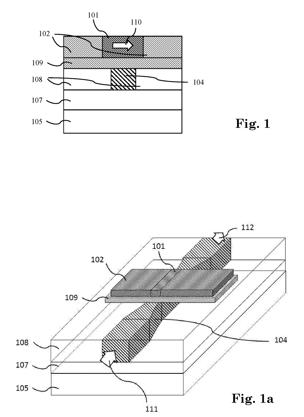
[0062]FIG. 1 shows a cross-sectional view illustrating an example of an electro-optic element, more particularly of a dielectrically loaded metal-insulator-metal plasmonic waveguide based ferroelectric material integrated plasmonic phase modulation element according to a first embodiment. The figure is taken in a transect plane perpendicular to the waveguide propagation direction. FIG. 1a is a perspective view of the electro-optic element of FIG. 1.

[0063]On a substrate or substrate layer 105, further layers and structures are provided, in particular by epitaxial growth, i.e. a buffered insulator layer 107 and a top device layer in which a core 104 (“second core”) of an optical waveguide (“second waveguide”) is structured. The material at 108 of the device layer adjacent to core 104 has a lower refractive index than that of the core 104 at the device operating wavelengths, i.e. at the wavelength of light guided in the second waveguide to be coupled, at least in part, into a first (pl...

second embodiment

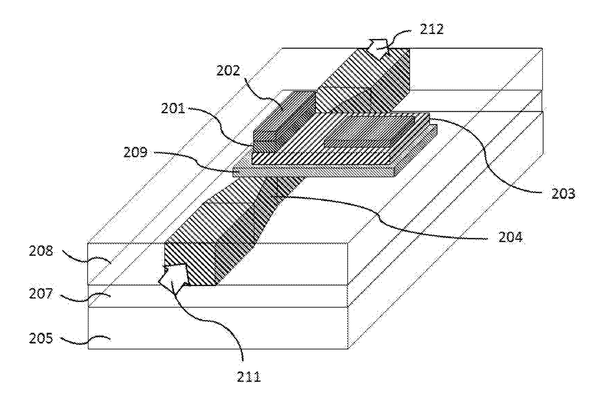
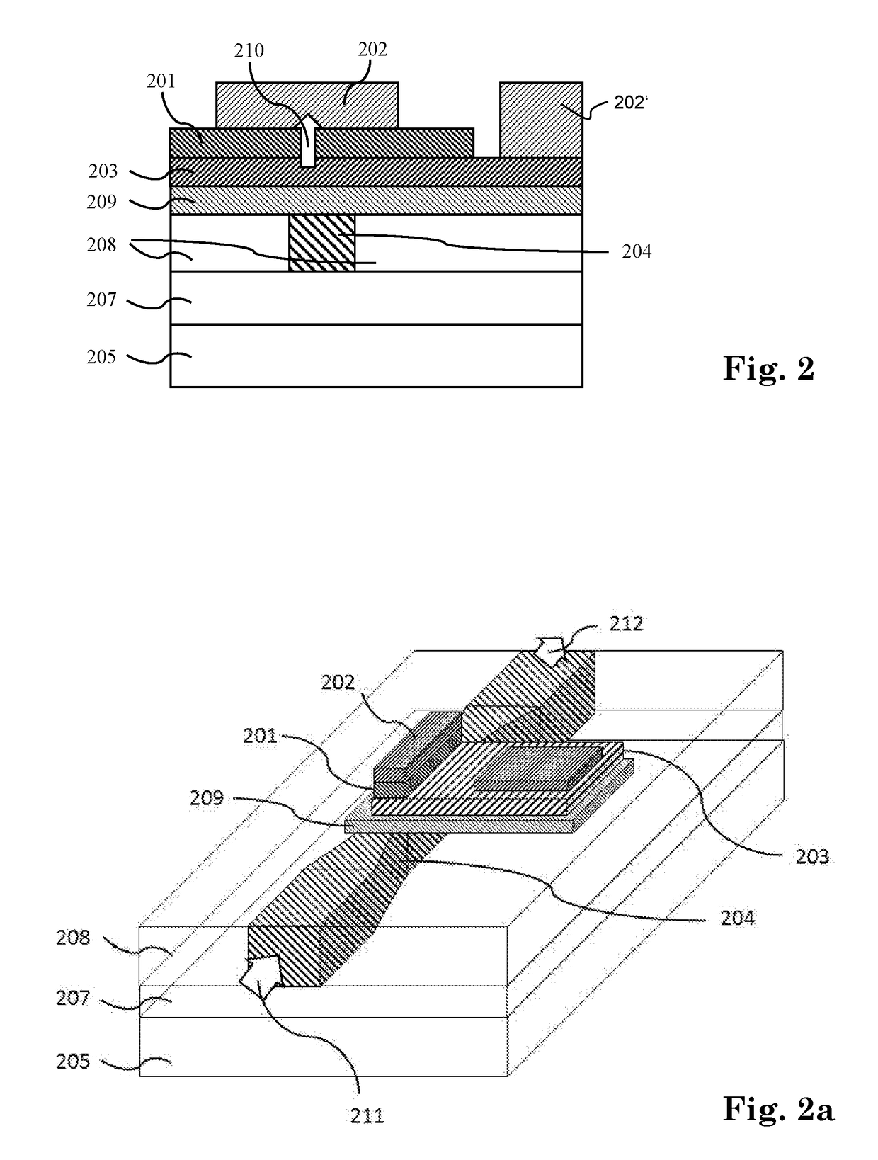
[0065]FIG. 2 shows a cross-sectional view illustrating an example of a dielectrically loaded metal-insulator plasmonic waveguide based ferroelectric material integrated plasmonic phase modulation element according to a second embodiment of the invention. The figure is taken in a transect plane perpendicular to the waveguide propagation direction. FIG. 2a is a perspective view of the electro-optic element of FIG. 2.

[0066]As shown in FIG. 2, this embodiment is different from the phase modulation element of the first embodiment in the formation of the plasmonic waveguide (first waveguide, ferroelectric core at 201) and applied electric field direction 210. Specifically, an electrically conductive material 203, which in particular may be non-metallic, is deposited on top of the layer stack including substrate 205 and buffered insulator 207 and a device layer with the second waveguide having a higher refractive index core 204 than the buffered insulator layer 207 beneath (e.g. Si core 20...

third embodiment

[0067]FIG. 3 shows a cross-sectional view illustrating an example of an oxide substrate-based ferroelectric material integrated plasmonic phase modulation element in a horizontal metal-insulator-metal plasmonic waveguide structure according to a third embodiment of the invention. This embodiment, an oxide substrate 306 is employed, such as MgO, Al2O3, SrTiO3, and LaSrAlTaO6. The choice of substrate materials is not limited to the aforementioned materials. Substrate materials that assist epitaxial growth of the ferroelectric material 301 and possesses a smaller refractive indices (real part) than the ferroelectric material 301 are preferred. Buffer layers and / or seed layers 309 can be introduced if necessary. Ferroelectric materials 301 are laterally sandwiched by metals 302, which are used as lateral cladding materials. Hence, surface plasmon polariton modes are supported. Guided modes are tightly confined in the ferroelectric materials 301 that are used as the core of the plasmonic...


PUM


Abstract

An electro-optic element includes a first waveguide, which is a plasmonic waveguide, including a first core having a ferroelectric material and a cladding having a first cladding portion. The first cladding portion includes, at a first interface with the ferroelectric material, a first cladding material. The electro-optic element includes a first and a second electrode for producing an electric field in the ferroelectric material when a voltage is applied between the first and second electrodes, for modulating a real part of a refractive index of the ferroelectric material. The element includes, in addition, a crystalline substrate on which the ferroelectric material is epitaxially grown with zero or one or more intermediate layers present between the substrate and the ferroelectric material. The element may have a second waveguide, which is a photonic waveguide, including for enabling evanescent coupling between the first and second waveguides.

Description

BACKGROUND OF THE INVENTIONField of the Invention[0001]The invention relates to electro-optic elements and to optical modulators including the same. It relates to electro-optic phase modulation and devices for enabling optical phase, amplitude and intensity modulation. The elements, devices and modulators may find application, e.g., in optical data- and telecommunications, optical storage and optical sensing.Description of Related Art[0002]Electro-optic modulators, which are used to encode information of electrical data in an optical signal, are key components in photonic links. The requirements of these devices are high speed, low energy consumption, low optical loss, high modulation depth, compact footprint, and dense integration. So far, optical modulators based on functional materials of compound semiconductors, liquid crystals, LiNbO3, or polymer, have been put into practical use. However, these optical modulators are commonly discrete and bulky, which is a consequence of the d...

Claims


Application Information

Patent Timeline
IPC IPC(8): G02F1/035G02F1/00G02F1/225
CPCG02F1/035G02F1/0027G02F1/225G02F2001/212G02F2203/10G02F2001/213G02F1/0508G02F1/212G02F1/213
Inventor MA, PINGLEUTHOLD, JURG
Owner ETH ZZURICH
Why Eureka
Try Eureka