Magnetoresistance effect element and magnetic memory device

a magnetic memory device and resistance effect technology, applied in the field of magnetic memory device and resistance effect element, can solve the problems of difficult to ensure the stable operation of the element, failure of the element, breakage or shrinkage of metal wiring, etc., and achieve the effect of reducing the width of the magnetic nanowire, reducing the adverse effect of joule heat generation, and reducing the current density

Active Publication Date: 2018-04-19
TOHOKU UNIV
View PDF4 Cites 6 Cited by
  • Summary
  • Abstract
  • Description
  • Claims
  • Application Information

AI Technical Summary

Benefits of technology

[0081]The hard axis anisotropic magnetic field HK⊥ is the size of the magnetic field that represents the difference in energy when the magnetization direction of the domain wall is oriented to the two directions other than the magnetic easy axis.
[0082]In the early stage of the study on the current induced domain wall movement, an NiFe alloy having the magnetization easy axis in the in-plane direction was often used. In the researches at that time, the width of the NiFe magnetic nanowire was in the 100 nm order, and the film thickness was in the 10 nm order. In this case, the domain wall width δw is about 100 nm. The hard axis anisotropic magnetic field HK⊥ corresponds to a difference in energy between the case in which the magnetization direction of the domain wall coincides with the Y axis direction as shown in FIG. 7A and the case in which the magnetization direction of the domain wall coincides with the Z axis direction as shown in FIG. 7B. In other words, the hard axis anisotropic magnetic field HK⊥ represents the difference between the state in which the magnetization appears on the δw×t plane (FIG. 7A) and the state in which the magnetization appears on the δw×w plane (FIG. 7B). In this case, the logical threshold current density obtained through calculation is in the order of 1013 to 1014 A / m2. However, it is not possible to provide a current with such a large current density to the element, and if a current density is smaller than this, the joule heat generation would occur, which would make the element operation unstable.
[0083]WO2009 / 001706 proposes the use of the vertical magnetization method instead of the in-plane magnetization method as a solution to the problem described above. In the vertical magnetization method, the film thickness is set to several nm, and the domain wall width δw is set to about 10 nm. The hard axis anisotropic magnetic field HK⊥ corresponds to a difference in energy between the case in which the magnetization direction of the domain wall coincides with the Y axis direction as shown in FIG. 7C and the case in which the magnetization direction of the domain wall coincides with the Z axis direction as shown in FIG. 7D. In other words, the hard axis anisotropic magnetic field HK⊥ represents the difference between the state in which the magnetization appears on the δw×t plane (FIG. 7C) and the state in which the magnetization appears on the w×t plane (FIG. 7D). In this case, the logical threshold current density obtained through calculation is in the order of 1011 A / m2. This mitigates the adverse effect of the joule heat generation, and it was confirmed that this configuration can achieve a desired domain wall movement property.
[0084]However, even in the vertical magnetization method, if the wire width of the magnetic nanowire was further reduced, the domain wall movement with a low current density would not be achieved. If the wire width w is greater than the domain wall width, Bloch domain wall is formed as shown in FIG. 7C, but if the wire width w is smaller than the domain wall width, Nair domain wall is formed as shown in FIG. 7D, and as the difference between the wire width w and the domain wall width increases, the hard axis anisotropic magnetic field HK⊥ increases.
[0085]FIGS. 8A to 8D show the results of the micromagnetic simulation with various magnetic nanowire widths w for the respective film thicknesses t of 2, 4, and 6 nm when the vertical magnetization method is employed.
[0086]Specifically, FIG. 8A shows the dependency of the domain wall width parameter Δ on the magnetic nanowire width w and the film thickness t. In this example, the value of the domain wall parameter Δ corresponding to the wire width w and the film thickness t was obtained. The wire width w was made to vary at a certain interval in a range from 10 nm to 100 nm during the simulation. The same applies to FIGS. 8B to 8D.

Problems solved by technology

When a magnetic layer having in-plane magnetization is used as described in Japanese Patent Application Laid-open Publication No. 2005-191032, the current density required for data writing (threshold current density) increases, and due to the breakage or shrinkage of metal wiring caused by Joule heat generation, it is difficult to ensure the stable operation of the element.
This results in a failure of the element such as breakage or shrinkage of the metal wiring.

Method used


Image

  • Magnetoresistance effect element and magnetic memory device
  • Magnetoresistance effect element and magnetic memory device
  • Magnetoresistance effect element and magnetic memory device

Examples


embodiment 1

[0029]Below, a magnetoresistance effect element of Embodiment 1 will be explained with reference to FIGS. 1 to 4.

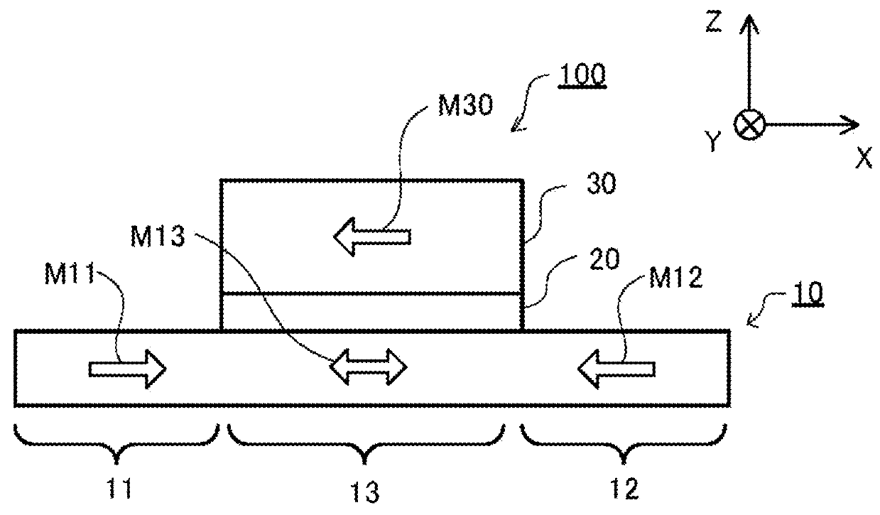
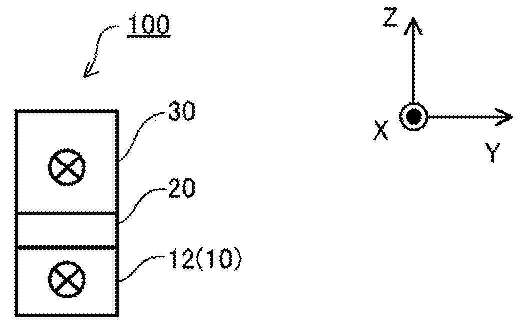
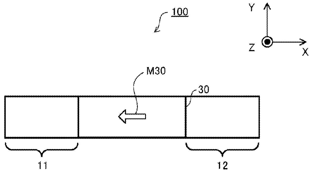
[0030]A magnetoresistance effect element 100 of Embodiment 1 includes a recording layer 10, a barrier layer 20, and a reference layer 30 stacked in this order as shown in the front view of FIG. 1A, the side view of FIG. 1B, and the plan view (top view) of FIG. 1C. In this embodiment, the lengthwise direction (extending direction) of the recording layer 10 (the direction toward right in FIG. 1A) is the X axis direction, the widthwise direction (the direction toward back in FIG. 1A) of the recording layer10 is the Y axis direction, and the height direction along which the respective layers of the magnetoresistance effect element 100 are stacked (the direction toward top in FIG. 1A) is the Z axis direction.

[0031]The recording layer 10 is made of a ferromagnetic body including an element such as Fe, Co, or Ni. Specifically, the recording layer 10 is made of a 3d transition me...

embodiment 2

[0109]In order to stably write and read data into and from the magnetoresistance effect element 100 of Embodiment 1, it is necessary to secure the magnetization direction M30 of the reference layer 30. In order to secure the magnetization direction M30 of the reference layer 30, it is effective to form the reference layer 30 of a multi-layer ferromagnetic coupling layer.

[0110]Below an embodiment of a magnetoresistance effect element 101 in which the reference layer 30 is made of a multi-layer ferromagnetic coupling layer will be explained with reference to FIG. 11.

[0111]In Embodiment 2, the reference layer 30 includes a ferromagnetic layer 31, a coupling layer 32, and a ferromagnetic layer 33, which forming a multi-layer structure with ferromagnetic coupling. The ferromagnetic layer 31 and the ferromagnetic layer 33 are coupled with each other via the coupling layer 32 in an anti-ferromagnetic manner. It is preferable to use a ferromagnetic material such as Fe, Co, and NI for the fe...

modification example 1

[0115]The combination of the resistance levels and data types can be appropriately changed, and it is also possible to assign the data “1” to the low resistance state and the data “0” to the high resistance state.


PUM


Abstract

A magnetoresistance effect element includes a recording layer containing a ferromagnetic body, and including a first fixed and second magnetization regions having magnetization components fixed substantially in a direction antiparallel to the in-plane direction to each other, and a free magnetization region disposed between the first and second fixed magnetization regions and having a magnetization component invertible in the in-plane direction, a domain wall disposed between the first fixed magnetization region and the free magnetization region, and being movable within the free magnetization region, and a magnetic nanowire having a width of 40 nm or less. The thickness of the recording layer is 40 nm or less and at least half but no more than twofold the width of the magnetic nanowire. The element further includes a barrier layer disposed on the recording layer, and a reference layer disposed on the barrier layer and containing a ferromagnetic body.

Description

BACKGROUND OF THE INVENTIONTechnical Field[0001]The present invention relates to a magnetoresistance effect element and magnetic memory device.Background Arts[0002]STT-MRAM (spin-transfer torque magnetic random access memory) using an MTJ (magnetic tunneling junction) element is drawing attention as the next generation non-volatile memory with high-speed and high-rewriting resistance capabilities. When data is written in the STT-MRAM, the resistance state of the MTJ element is changed to a high resistance state or low resistance state using spin transfer torque (STT), and stored data is read out by detecting the resistance state of the MTJ element.[0003]The data writing methods of STT-MRAM include the spin injection magnetization inversion method, and the current induced magnetization method. In the spin injection magnetization inversion method, an electric current is introduced to a magnetoresistance effect element, and by using the torque generated by spin polarized electrons to m...

Claims


Application Information

Patent Timeline
Patent Type & Authority Applications(United States)
IPC IPC(8): G11C11/02H01L43/08G11C7/10G01R33/09
CPCG11C11/02H01L43/08G11C7/10G01R33/093B82Y25/00B82Y10/00G11C11/1659G01R33/098G11C11/161G11C11/1673G11C11/1675H01F1/0072H01F10/3254H10N50/10
Inventor FUKAMI, SHUNSUKEIWABUCHI, TORUOHNO, HIDEOENDOH, TETSUO
Owner TOHOKU UNIV
Why Eureka
Try Eureka