Transparent and electrically conductive coatings containing non-stoichiometric metallic nitrides

a technology of metallic nitrides and transparent coatings, which is applied in the direction of photomechanical treatment originals, vacuum evaporation coatings, instruments, etc., can solve the problems of inability to guarantee surface variations below 1 nm, increasing the complexity of photolithographic mask manufacturing, and increasing the cost of production

Inactive Publication Date: 2018-06-07
FUNDACIO INST DE CIENCIES FOT NIQUES +1
View PDF0 Cites 0 Cited by
  • Summary
  • Abstract
  • Description
  • Claims
  • Application Information

AI Technical Summary

Benefits of technology

[0016]In a first embodiment, the present invention is directed to a composition for a photolithographic mask comprising a substrate; and a coating deposited on a surface of the substrate, the coating comprising at least one electrical conducting layer comprising a thickness from about 5 nm to about 30 nm; and at least one metal nitride of the formula MNy, wherein M is a metal comprising Cr, Ti, Al, Si or combinations thereof, N is nitrogen, and y is greater than zero and less than 1. In some embodiments, the at least one electrical conducting layer has an optical transmittance from about 5% to about 35% in the wavelength range of 300 nm to 1600 nm. In some embodiments, the at least one electrical conducting layer has a sheet resistance from about 70 Ω / □ to about 200 Ω / □. In other embodiments, the at least one electrical conducting layer comprises a metal oxynitride having the general formula MOxNy, wherein M, N and y are defined as above, O is oxygen, and x is greater than zero and less than 1. In other embodiments, the at least one electrical conducting layer has a thickness that varies less than ±5% across the at least one electrical conducting layer. In other embodiments, the at least one electrical conducting layer comprises a surface roughness of ≤0.6 nm route mean square across an area of up to 100 μm2. In other embodiments, the substrate comprises fused silica, ZERODUR®, ULE® or CLEARCERAM®.
[0017]In a second embodiment, the present invention is a method of making a composition for a photolithographic mask comprising the steps of providing a substrate; and depositing a coating on the substrate, the coating comprising at least one electrical conducting layer having a thickness less than 50 nm, and at least one metal nitride of the formula MNy, wherein M is a metal comprising Cr, Ti, Al, Si or combinations thereof, N is nitrogen, and y is greater than zero and less than 1. In some embodiments, the coating is deposited on the substrate by physical vapor deposition. In other embodiments, the physical vapor deposition method comprises a reactive deposition. In other embodiments, the physical vapor deposition method occurs in a chamber having a pressure of from about 9.9×10⁻⁷ Torr to about 1×10⁻⁷ Torr. In other embodiments, the step of adjusting the temperature of the substrate from about 100° C. to about 150° C. In other embodiments, the coating is deposited onto the substrate comprising a thermal evaporation process. In other embodiments, the coating is deposited onto the substrate comprising a chemical vapor deposition.
[0018]In some embodiments, a method of the present invention further comprises providing a flow of argon gas and a flow of nitrogen gas to the composition; and adjusting the flow of argon gas and the flow nitrogen to vary the amount of nitrogen present in the metal nitride. In other embodiments, the total flow of argon and nitrogen gas is about 20 sccm. In other embodiments, the flow of argon gas is from about 11 sccm to about 19 sccm and the flow of nitrogen gas is about 1 sccm to about 9 sccm. In some embodiments, the method further comprises providing a flow of oxygen gas to the composition; and forming a metal oxynitrides having the formula MOxNy, wherein M, N and y are defined as above, O is oxygen, and x is greater than zero and less than 1.

Problems solved by technology

As a consequence, the manufacturing of photolithographic masks with increasing resolution is becoming more and more complex, and thus more and more expensive as well.
However, even the best production techniques cannot guarantee surface variations below 1 nm.
Moreover, the fabrication of mask blanks and / or EUV optical elements from mask blanks may additionally induce further defects in the EUV substrates, and / or thus also in the EUV optical elements.
Moreover, defects may evolve in the course of the operation of an EUV mask in a lithography system.
The trade-off between Rs and T for CrN is such that it cannot meet the typical electrical requirements of lithomask if the coating has to be transparent.
However, Cr is not as strong as CrN from a mechanical resistance (hardness) point of view, for example against sliding, scratching and abrasive forces.
However due to the intrinsic mechanical weakness of Cr and the difference in thermal and mechanical properties of the two materials (Cr and CrN), adhesion problems may occur.

Method used


Image

  • Transparent and electrically conductive coatings containing non-stoichiometric metallic nitrides
  • Transparent and electrically conductive coatings containing non-stoichiometric metallic nitrides
  • Transparent and electrically conductive coatings containing non-stoichiometric metallic nitrides

Examples


examples

[0048]In the following, the present invention will now be described in more detail hereinafter with reference to the accompanying figures, in which exemplary embodiments of the invention are illustrated. However, the present invention may be embodied in different forms and should not be construed as limited to the embodiments set forth herein. Rather, these embodiments are provided so that this disclosure will be thorough and will convey the scope of the invention to persons skilled in the art.

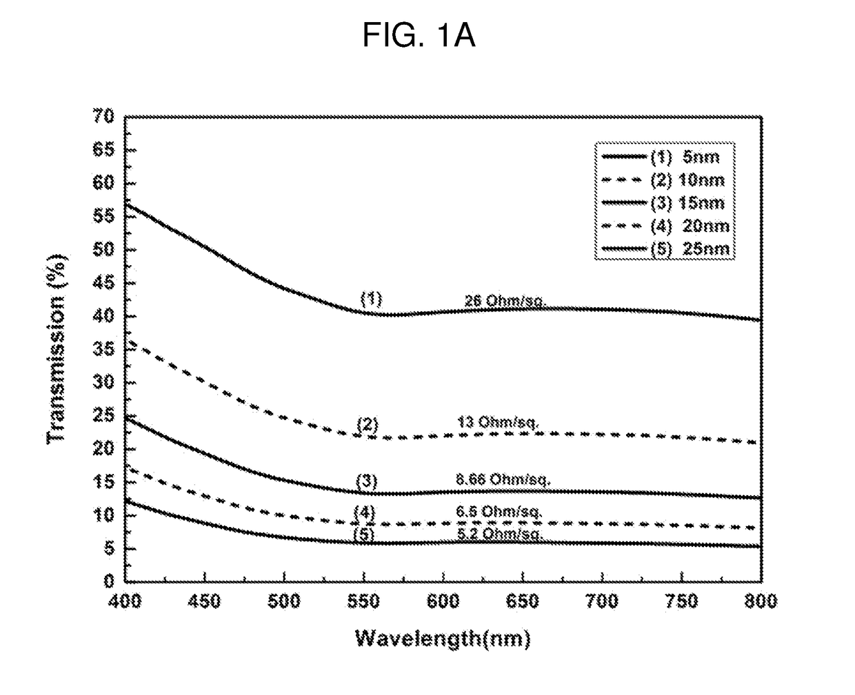
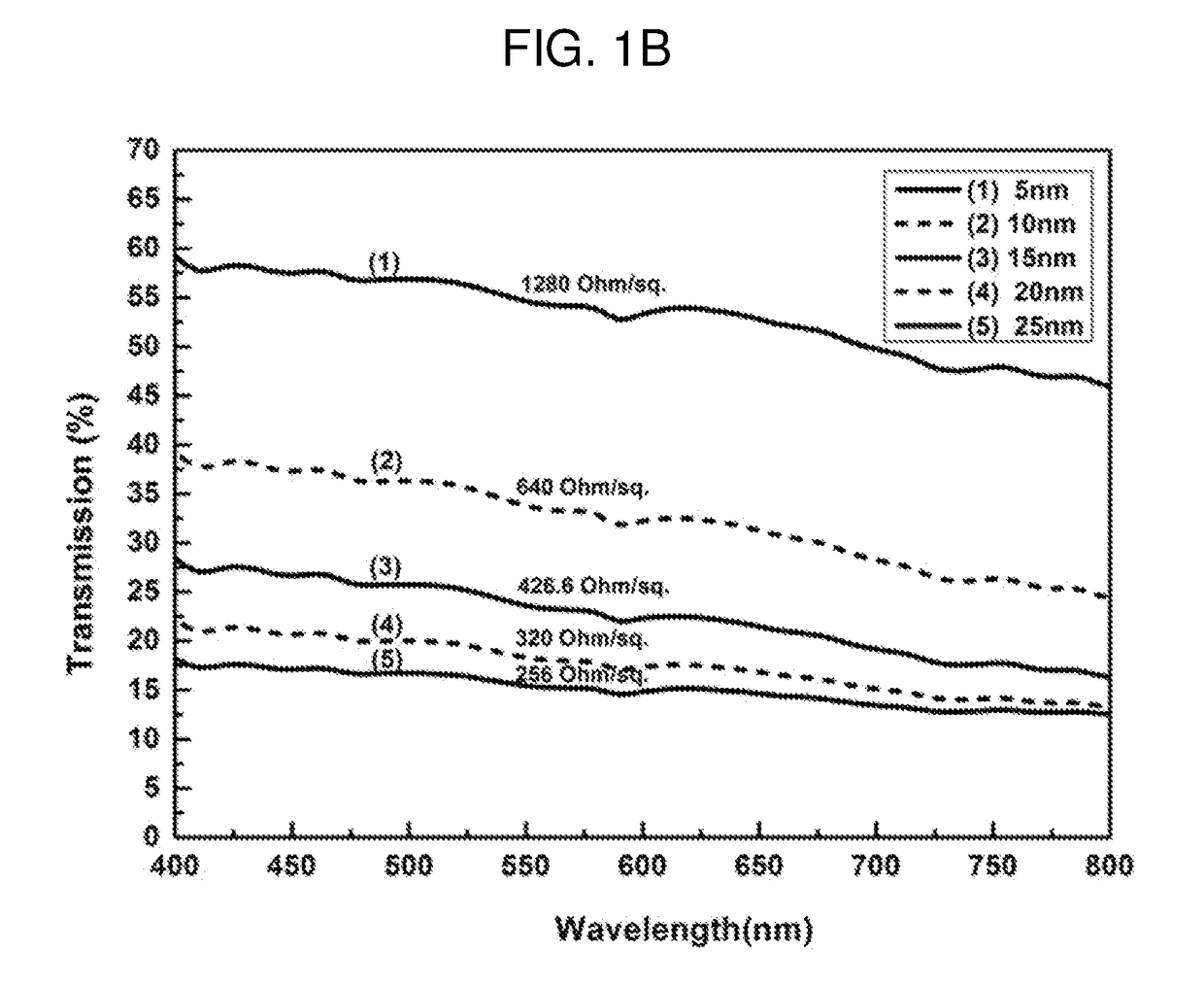
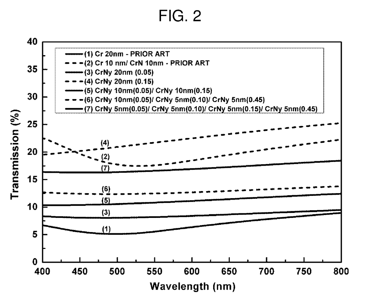
[0049]A double side optically polished UV fused silica glass with 1 mm thickness and 1 inch square was used as substrate. Before deposition of the coating, the substrates were cleaned in acetone followed by ethanol in ultrasonic bath, each process lasting 10 min. The substrate was then rinsed in DI water and dried with nitrogen gas followed by argon plasma cleaning for 15 min inside the sputtering machine. 20 sccm of Argon gas with 8 mT pressure and 40W BIAS power was used for plasma cleaning....


PUM

PropertyMeasurementUnit
thicknessaaaaaaaaaa
optical transmittanceaaaaaaaaaa
surface roughnessaaaaaaaaaa

Abstract

The present invention is directed to compositions for photolithographic masks comprising a substrate and a coating having at least one electrical conducting layer comprising a metal nitride of the formula MNy, wherein M is a metal and y is greater than zero and less than 1, and methods of making the same.

Description

FIELD OF THE INVENTION[0001]The present invention relates to the field of optically transparent and electrically conductive coatings on a substrate. In particular semi-transparent backside coatings of lithography masks.BACKGROUND OF THE INVENTION[0002]As a result of the constantly increasing integration density in the semiconductor industry, photolithographic masks have to project smaller and smaller structures. In order to fulfil this demand, the exposure wavelength of photolithographic masks has been shifted from the near ultraviolet across the mean ultraviolet into the far ultraviolet region of the electromagnetic spectrum. Presently, a wavelength of 193 nm is typically used for the exposure of the photoresist on wafers. As a consequence, the manufacturing of photolithographic masks with increasing resolution is becoming more and more complex, and thus more and more expensive as well. In order to use significantly smaller wavelengths, lithography systems for the extreme ultraviol...

Claims


Application Information

Patent Timeline
Patent Type & Authority Applications(United States)
IPC IPC(8): G03F1/38G03F1/22C23C14/06C23C14/24C23C16/34C23C16/30
CPCG03F1/38G03F1/22C23C14/0641C23C14/0676C23C16/34C23C16/308C23C14/24G03F1/40
Inventor PRUNERI, VALERIOMANIYARA, RINU ABRAHAM
Owner FUNDACIO INST DE CIENCIES FOT NIQUES
Why Eureka
Try Eureka