
Variable resistance element and method for producing variable resistance element

a technology of resistance element and variable resistance, which is applied in the field of variable resistance element, can solve the problems of increasing the price of manufacturing tools and mask sets, increasing the cost of lithography process,

Active Publication Date: 2018-06-14
NANOBRIDGE SEMICON INC
View PDF2 Cites 6 Cited by
  • Summary
  • Abstract
  • Description
  • Claims
  • Application Information

AI Technical Summary

Benefits of technology

The present invention provides a variable resistance element that stabilizes the second electrode and improves the dielectric breakdown voltage when a reset voltage is applied.

Problems solved by technology

The increase in lithography process costs includes increase in the price of manufacturing a tool and the price of mask sets.

Method used


Image

  • Variable resistance element and method for producing variable resistance element
  • Variable resistance element and method for producing variable resistance element
  • Variable resistance element and method for producing variable resistance element

Examples


first example embodiment

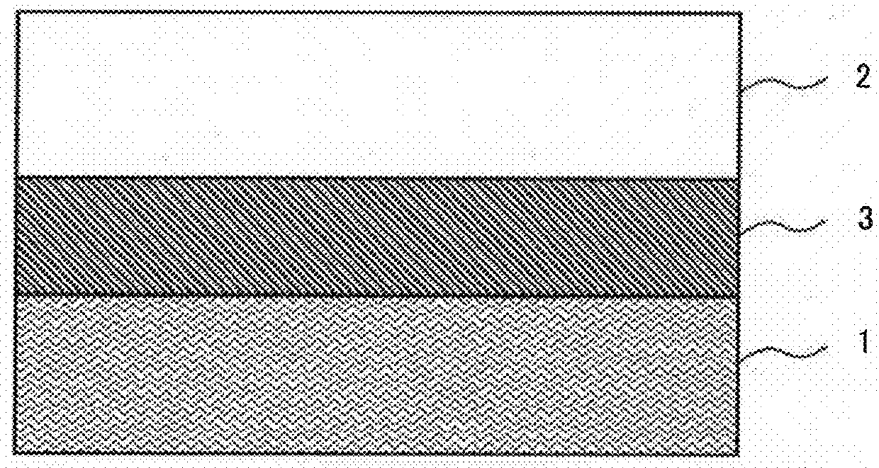
[0042]A variable resistance element according to a first example embodiment of the present invention will be described by using a drawing. FIG. 1 is a cross-sectional view schematically illustrating a variable resistance element according to the first example embodiment of the present invention. FIG. 1 is a cross-sectional view schematically illustrating a configuration example of a semiconductor device of the present example embodiment.

[0043]As illustrated in FIG. 1, the variable resistance element of the present example embodiment includes a first electrode 1, an ion conducting layer 3 and a second electrode 2. In the variable resistance element in FIG. 1, the ion conducting layer 3 and the second electrode 2 are formed on the first electrode 1 in order. The first electrode 1 is made of metals including copper (Cu) and may be made primarily of copper (Cu). The ion conducting layer 2 contains elements of silicon (Si), oxygen (O) and carbon (C) as materials.

[0044]The first electrode...

second example embodiment

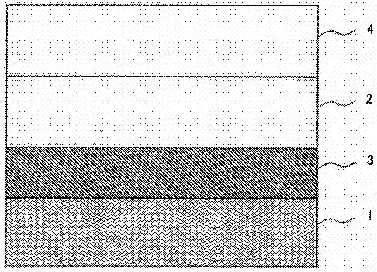
[0052]A variable resistance element according to a second example embodiment of the present invention will be described next by using a drawing. FIG. 2 is a cross-sectional view schematically illustrating a variable resistance element according to the second example embodiment of the present invention.

[0053]Like the variable resistance element in FIG. 1, the variable resistance element in FIG. 2 includes a first electrode 1, an ion conducting layer 3 and a second electrode 2. The variable resistance element in FIG. 2 further includes a third electrode 4 that is in contact with the second electrode 2 and is not in contact with the ion conducting layer 3. The third electrode 4 is characterized by containing at least the first metal described above and nitrogen.

[0054]The third electrode 4 of the present example embodiment serves to protect the second electrode 2 from damage caused by etching in a production process of the variable resistance element. When the second electrode 2 is fabr...

example 1

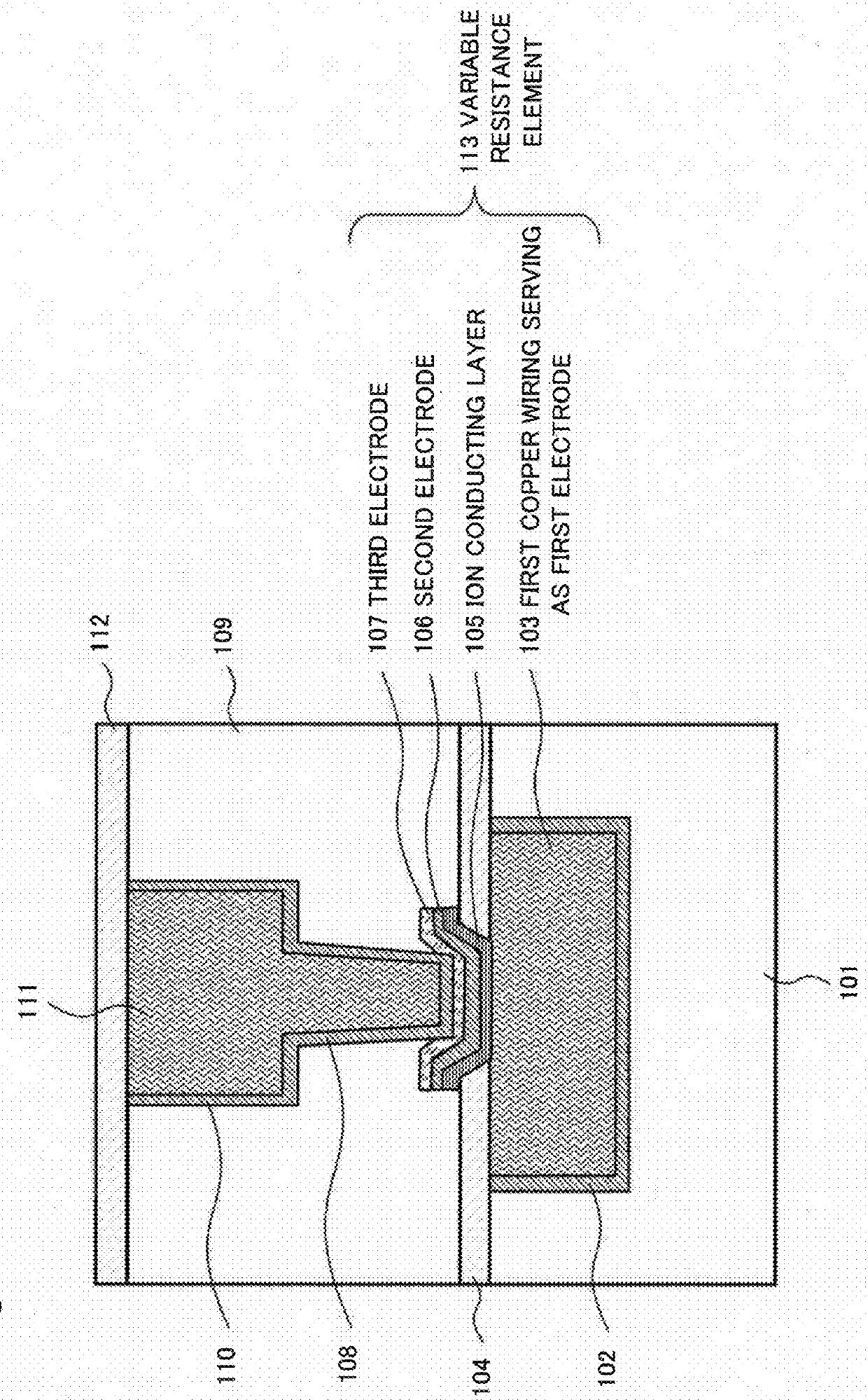
[0060]As more specific example embodiments of the present invention, examples will be described below. FIG. 3 is a cross-sectional view schematically illustrating a semiconductor device in which a variable resistance element according to the first example embodiment of the present invention is formed. The semiconductor device in FIG. 3 includes a first interlayer insulating film 101, a barrier metal 102, a first copper wiring 103 serving as a first electrode, a first insulating barrier film 104, an ion conducting layer 105, a second electrode 106, a third electrode 107, and a copper plug 108. The semiconductor device in FIG. 3 further includes a second interlayer insulating film 109, a barrier metal 110, a second copper wiring 111, and a second insulating barrier film 112.

[0061]The variable resistance element of the semiconductor device in FIG. 3 includes a first electrode formed in the first interlayer insulating film 101 on a semiconductor substrate (not depicted). The first elect...


PUM


Abstract

In order to improve the number rewrites by improving the dielectric breakdown resistance of an ion conducting layer in a variable resistance element, this variable resistance element is provided with: a first electrode that contains at least copper; a second electrode that contains at least Ru, nitrogen and a first metal; and an ion conducting layer that is positioned between the first electrode and the second electrode.

Description

TECHNICAL FIELD[0001]The present invention relates to a variable resistance element and a method for producing a variable resistance element and, in particular, to a variable resistance element in which one electrode contains a ruthenium and a method for producing the variable resistance element.BACKGROUND ART[0002]A semiconductor device including a silicon device has been advancing in integration and decreasing in power consumption due to miniaturization according to the scaling law known as Moore's law and have been developed at such a rate that “integration will be quadrupled in three years”. A gate length of Metal Oxide Semiconductor Field Effect Transistor (MOSFET) has been reduced to 20 nm or less in recent years. Because of increase in lithography process costs and physical limits of device dimensions caused by this, device performance improvement by an approach different from the existing scaling law is demanded.[0003]The increase in lithography process costs includes increa...

Claims


Application Information

Patent Timeline
Patent Type & Authority Applications(United States)
IPC IPC(8): H01L45/00H10N99/00
CPCH01L45/1266H01L45/085H01L45/1233H10N70/245H10N70/841H10N70/8416H10N70/881H10N70/826H10N70/8833G11C2213/51H10N70/883H10N70/24H10N70/8265
Inventor TADA, MUNEHIROBANNO, NAOKIOKAMOTO, KOICHIRO
Owner NANOBRIDGE SEMICON INC
Learn More