Arylamine compound and organic electroluminescent device
a technology of organic electroluminescent devices and arylamine compounds, which is applied in the direction of luminescent compositions, organic chemistry, chemistry apparatus and processes, etc., can solve the problems of low heat resistance, material deterioration, and confinement of excitons generated within the luminous layer, and achieve excellent electron blocking capability, excellent heat resistance, and high hole mobility
- Summary
- Abstract
- Description
- Claims
- Application Information
AI Technical Summary
Benefits of technology
Problems solved by technology
Method used
Image
Examples
example 1
Device Example 1
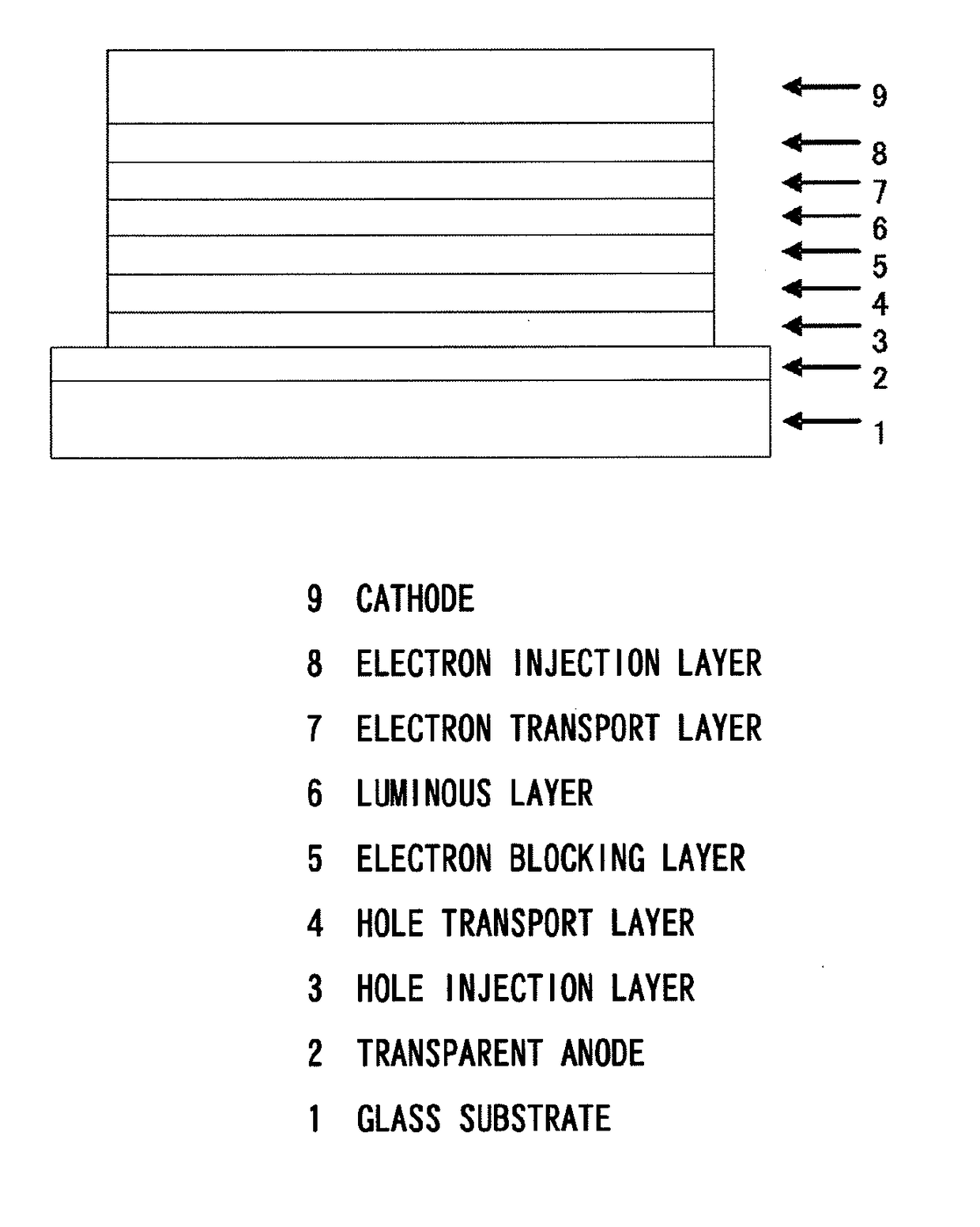
[0352]The hole injection layer 3, the hole transport layer 4, the electron blocking layer 5, the luminous layer 6, the electron transport layer 7, the electron injection layer 8, and the cathode (aluminum electrode) 9 were vapor-deposited in this order on an ITO electrode formed beforehand as the transparent anode 2 on the glass substrate 1 to prepare the organic EL device as shown in FIG. 11.
[0353]Concretely, the glass substrate 1 having a 50 nm thick ITO film formed thereon was washed with an organic solvent, and then the ITO surface was cleaned by UV / ozone treatment. Then, the glass substrate with the ITO electrode was placed in a vacuum deposition machine, and the pressure therein was reduced to 0.001 Pa or lower.
[0354]The hole injection layer 3 was formed. Concretely, a compound HIM-1 represented by the following structural formula was vapor-deposited so as to cover the transparent anode 2, whereby a layer with a film thickness of 5 nm was formed.
[0355]Then, the...
example 2
Device Example 2
[0362]An organic EL device was prepared under the same conditions as in Device Example 1, except that the compound of Example 2 (Compound 10) was used, instead of the compound of Example 1 (Compound 2), as the material for the electron blocking layer 5.
example 3
Device Example 3
[0363]An organic EL device was prepared under the same conditions as in Device Example 1, except that the compound of Example 3 (Compound 41) was used, instead of the compound of Example 1 (Compound 2), as the material for the electron blocking layer 5.
PUM
| Property | Measurement | Unit |
|---|---|---|
| Volume | aaaaa | aaaaa |
| Volume | aaaaa | aaaaa |
| Volume | aaaaa | aaaaa |
Abstract
Description
Claims
Application Information


