Simultaneous Break and Expansion System for Integrated Circuit Wafers

a technology of integrated circuit wafers and expansion systems, applied in the direction of electrical equipment, semiconductor devices, metal working equipment, etc., can solve the problems of increasing the chance of breaking during later assembly steps or in actual use, reducing yield, and ic die strength reduction, etc., to reduce or eliminate die collisions

Inactive Publication Date: 2018-11-08
PSEMI CORP
View PDF19 Cites 4 Cited by
  • Summary
  • Abstract
  • Description
  • Claims
  • Application Information

AI Technical Summary

Benefits of technology

[0017]The invention encompasses improved methods for singulating integrated circuit (IC) dies that reduce or eliminate die collisions, work well with very small dies (e.g., less than about 1.0 mm on the shortest edge), and work

Problems solved by technology

Defects may include chipped IC die edges and stress fractures that reduce IC die strength and increase the chance of breaking during later assembly steps or in actual use.
For example, the presence of metal and/or TEGs within cutting streets generally prohibits use of cutting saws, since such in-street structures may clog a saw.
Rotary blade cutting and mechanical scribing can also cause die edge chipping or cracking, leading to lower yields, and both methods generally have relatively wide kerfs (e.g., greater than about 50 μm).
Backside metallization may prohibit use of certain laser-based methods, or pose cutter alignment problems.
Stealth dicing generally does not work for IC dies having in-street metal or TEGs on the patterned front side of a wafer substrate, since the subsurface modified layers do not cut the front-side structures, resulting in errant breaks in the metal and/or inability to separate dies.
A problem with the method of FIG. 1 is that it does not work well with very small dies (e.g., less than about 1.0 mm on the shortest edge).
In addition, when the expansion tension is released, if the dicing tape has not yielded under expansion, the dicing tape memory will pull the dies back together, which may cause damaging die collisions.
Alternatively, when the expansion tension is released, if the dicing tape has yielded, the dicing tape becomes slack, which again may cause damaging die collisions.
In a variant of the process depicted in FIG. 1, the singulation process may be conducted in a cooling chamber, which aids in singulating smaller die, but still suffers the problem of allowing post-e

Method used


Image

  • Simultaneous Break and Expansion System for Integrated Circuit Wafers
  • Simultaneous Break and Expansion System for Integrated Circuit Wafers
  • Simultaneous Break and Expansion System for Integrated Circuit Wafers

Examples


Embodiment Construction

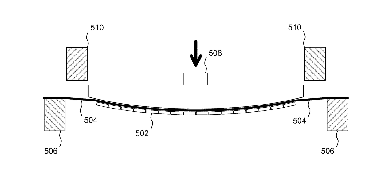
[0040]The invention encompasses improved apparatus and methods for singulating integrated circuit (IC) dies that reduce or eliminate die collisions, work well with very small dies (e.g., less than about 1.0 mm on the shortest edge), and work well with both uniform grid patterns die layouts and non-uniform grid pattern die layouts (e.g., multi-project wafers or multi-product wafers). Further, embodiments of the invention simultaneously separate dies in two dimensions.

[0041]Embodiments of the invention utilize a simultaneous break and expansion system for separating individual IC dies from a scored wafer substrate, and avoid die collisions by maintaining IC die separation once singulation has occurred. The system may use a variety of scored wafer substrates, and works well in particular with wafer substrates that have been both laser scribed and stealth diced in accordance with the teachings of co-pending U.S. patent application Ser. No. 15 / 432,838, referenced above.

[0042]Overview of ...


PUM

PropertyMeasurementUnit
Diameteraaaaaaaaaa
Dimensionaaaaaaaaaa
Tensionaaaaaaaaaa

Abstract

Improved methods and apparatuses for singulating integrated circuit (IC) dies that reduce or eliminate die collisions and work well with very small dies. Embodiments simultaneously separate dies in two dimensions by utilizing a break and expansion system that avoids die collisions by maintaining IC die separation after singulation. Singulation is achieved by placing the joined dies of the wafer substrate on a dicing tape, scoring the wafer substrate between the joined dies, and imposing a bending action by pressing a curved surface against the scored wafer substrate, which also expands the wafer substrate by stretching the dicing tape. After breaking, an inner expansion grip ring is pressed into an outer expansion grip ring in a nested configuration so as to maintain the stretched state of the dicing tape after the curved surface is fully removed, thereby maintaining the dicing tape in tension and the singulated die in spaced apart relation.

Description

CROSS-REFERENCE TO RELATED APPLICATIONS—CLAIM OF PRIORITY[0001]The present application claims priority to U.S. provisional Patent Application No. 62 / 500,420, filed on May 2, 2017, for a “Simultaneous Break and Expansion System for Integrated Circuit Wafers”, which is herein incorporated by reference in its entirety. This application may be related to U.S. patent application Ser. No. 15 / 432,838, filed Feb. 14, 2017, entitled “Wafer Dicing Methods”, assigned to the assignee of the present invention and hereby incorporated by reference.BACKGROUND(1) Technical Field[0002]This invention relates to methods for the singulation of integrated circuit dies from processed wafer substrates, also known as “wafer dicing”.(2) Background[0003]Integrated circuits (ICs) are almost universally fabricated as multiple units formed on round wafer substrates. Common wafer substrates include silicon, sapphire, silicon-on-insulator (SOI), silicon-on-sapphire (SOS), gallium arsenide, and various insulators (...

Claims


Application Information

Patent Timeline
IPC IPC(8): H01L21/78H01L21/683B26F3/00B28D1/22
CPCH01L21/78H01L21/6836B26F3/002B28D1/225B28D5/0011B28D5/0052H01L2221/68327
Inventor DEMAIORIBUS, VINCENTJAMES, JOHN
Owner PSEMI CORP
Why Eureka
Try Eureka