

Charged particle beam device and scanning electron microscope
a technology of scanning electron microscope and charge beam, which is applied in the direction of basic electric elements, electric discharge tubes, electrical apparatus, etc., can solve the problem that the first objective lens and the second objective lens cannot be operated simultaneously, and achieve the effect of improving performan
- Summary
- Abstract
- Description
- Claims
- Application Information
AI Technical Summary
Benefits of technology
Problems solved by technology
Method used
Image

Examples
embodiment 1
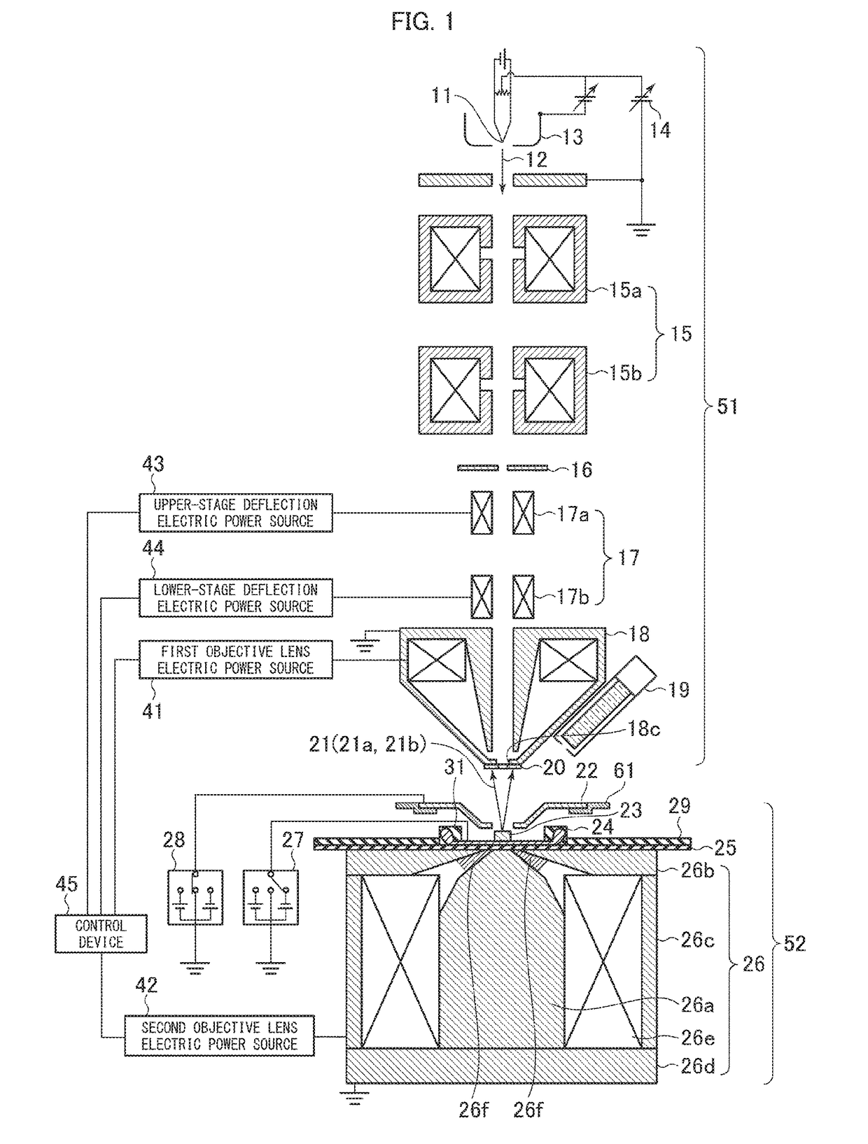
[0033]The description below deals with a schematic configuration of a SEM as Embodiment 1 of the present invention with reference to FIG. 1.
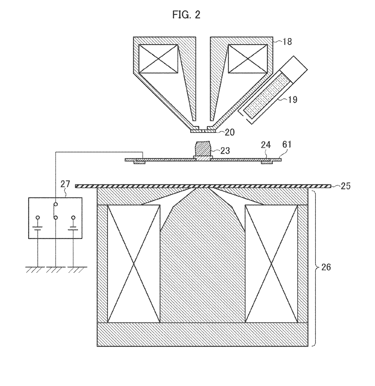
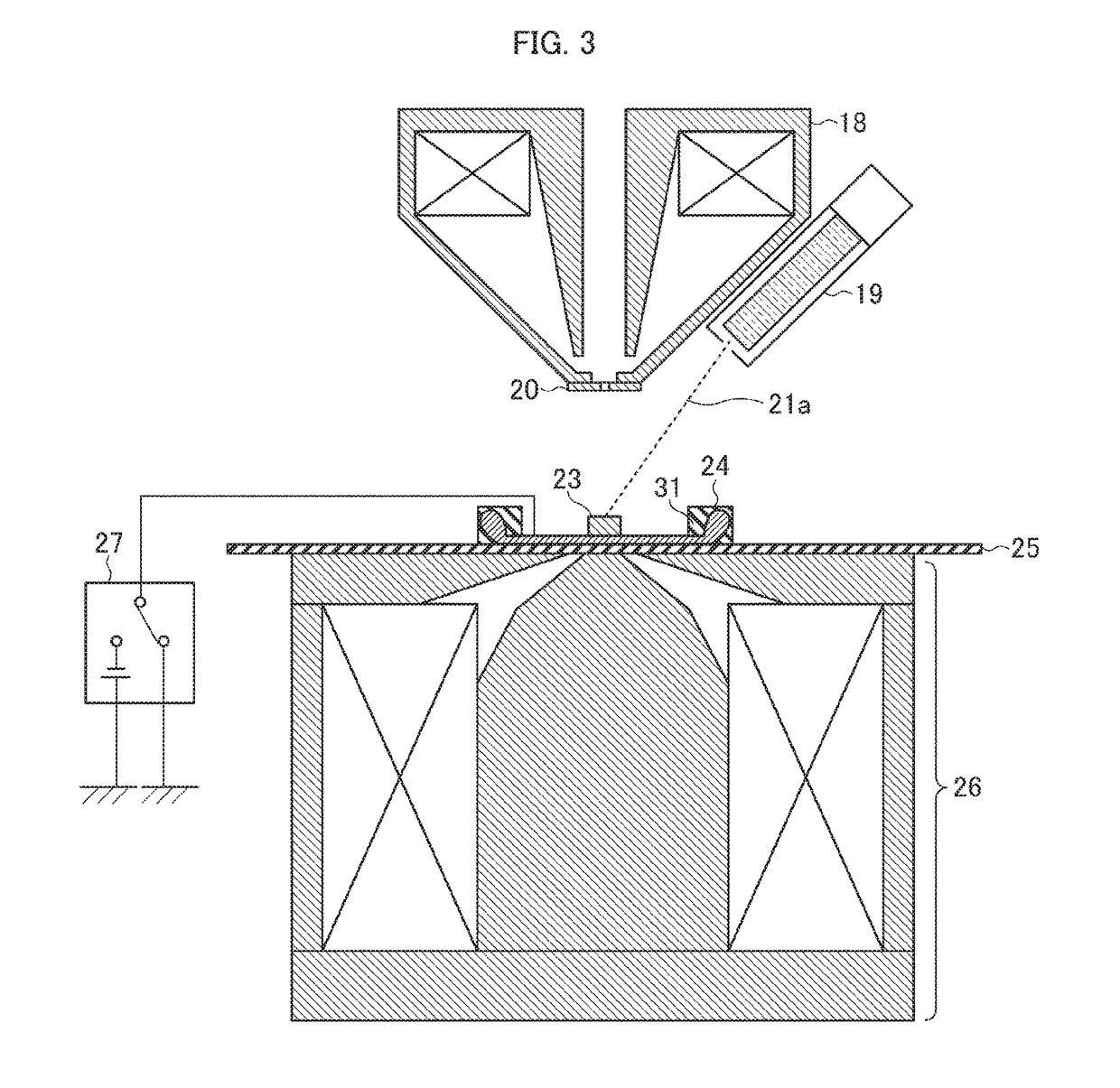
[0034]The SEM is an electron beam device including an electron source (charged particle source) 11, an acceleration electric power source 14, a condensing lens unit 15, an objective-lens aperture 16, a two-stage deflection coil unit 17, objective lenses 18 and 26, and a detector 20. The acceleration electric power source 14 accelerates a primary electron beam (charged particle beam) 12 emitted by the electron source 11. The condensing lens unit 15 focuses the accelerated primary electron beam 12. The objective-lens aperture 16 removes an unnecessary portion of the primary electron beam 12. The two-stage deflection coil unit 17 scans a sample 23 two-dimensionally with the primary electron beam 12. The objective lenses 18 and 26 focus the primary electron beam 12 onto the sample 23. The detector 20 detects signal electrons 21 (secondary electrons ...
embodiment 2
[0146]With reference to FIG. 8, the following description will discuss a simple device configuration that does not include a first objective lens 18.
[0147]This configuration includes a semiconductor detector 20 below the lower-stage deflection coil 17b. The absence of a first objective lens 18 allows the distance between the lower-stage deflection coil 17b and the second objective lens 26 to be smaller accordingly. A device configuration like this is suitable in terms of downsizing. The SEM of Embodiment 2 can be used in a manner similar to the SEM of Embodiment 1 except that a first objective lens 18 is not used in Embodiment 2. The detector 20 and the second objective lens 26 are separated from each other by a distance of 10 mm to 200 mm.
[0148]The members ranging from the electron source 11 to the lower-stage deflection coil 17b in the device illustrated in FIG. 8 constitute an upper unit 51 for causing a primary electron beam 12 to be emitted toward a sample 23. FIG. 8 also shows...
embodiment 3
[0149]Embodiment 3 uses an electron source of the field emission type as the electron source 11. An electron source of the field emission type, as compared to an electron source of the thermoelectronic emission type, has a high luminance, a small light source, a small ΔV for a primary electron beam 12, and an advantage in terms of chromatic aberration. Embodiment 3 is, for comparison with Embodiment 1, configured such that the second-stage condensing lens 15b and the members therebelow are identical to those of Embodiment 1, that the electron source section is of the field emission type, and that the first-stage condensing lens 15a is absent. The primary electron beam 12 has ΔV of 0.5 eV, and the electron source has a size So of 0.1 μm. The performance for a case where Z=−4 mm, the accelerating voltage Vacc is −30 kV, and the first objective lens 18 is unused is calculated as follows:
[0150](Simulation Data 7)
[0151]Dprobe=0.974 nm, Dg=0.071, Ds=0.591, Dc=0.248, Dd=0.730,
[0152]Cs=1.69...
PUM
 Abstract
Description
Claims
Application Information