Circuit Arrangement For Switching Noise Jitter (SNJ) Reduction In Feedback Control Loop Circuits, And Methods Of Making The Same

a feedback control loop and circuit arrangement technology, applied in the direction of electric variable regulation, process and machine control, instruments, etc., can solve the problems of short battery life, low conversion efficiency, and perceived supply bias noise, and achieve enhanced user experience and improved battery life without compromising maximum wireless and system performance.

Active Publication Date: 2019-02-28
TRANSSIP
View PDF0 Cites 3 Cited by
  • Summary
  • Abstract
  • Description
  • Claims
  • Application Information

AI Technical Summary

Benefits of technology

[0017]The present invention seeks to provide novel components, circuit topologies and associated methods for modifying the noise signature of control circuits and switching mode DC-DC converter circuits in which SNJ is a major contributor, particularly those circuits that include negative feedback loops and PFM conversions. This invention therefore enables the use of switching mode DC-DC converters in noise-sensitive circuits and electronics systems thereby achieving greater power conversion efficiencies and systems performance which is equal if not superior to that achieved by systems powered by linear regulators.
[0018]These goals are achieved, according to one embodiment of the invention, by providing a passive signal conditioning device comprising a substantial ESR coupled to a broadband attenuator. The passive signal conditioning device responds to an input alternating signal, increasing the slopes of the feedback signal ramps and decreasing the noise being carried thereon going into the control loop circuit and reducing time variability of the decision control (i.e. changing states from one to another) therein. The passive signal conditioning device reduces the amount of SNJ and overall noise characteristics on the output of the control circuit.
[0020]PFM DC-DC converters incorporating the disclosed passive signal conditioning device, the chaotic characteristics of supply bias noise represented by SNJ are no longer presented to powered circuit elements. Therefore the disclosed passive signal conditioning device in accordance with the present invention improves performance and noise of the output of PFM-type DC-DC converters. This enables use of PFM-type DC-DC converters to power noise-sensitive RF and microwave circuits and systems, as well as time domain functions such as clock circuits, oscillators, analog-to-digital converters, integrator, convolution of signals and the like. A further advantage of the present invention is the delivery of improved power conversion efficiency ranging from light load / standby to full load operation without degradation of overall supply bias noise and the stability of the regulated voltage under the influence of pulsed load conditions due to power saving operation modes.
[0022]Accordingly several advantages of one or more aspects are as follows: to reduce both time domain noise signature (i.e. SNJ) and frequency domain noise in control circuits suitable for use in negative feedback control loop circuitries, thereby enabling use of PFM DC-DC converters in noise-sensitive applications with the result that substantially longer battery life and performance equal or superior to linear regulator-powered systems is provided, and that can be suitable for ultra-low power switching mode DC-DC converter designs in that additional active circuit elements for noise reduction are not required. Other advantages of one or more aspects will be apparent from a consideration of the drawings and ensuing description.

Problems solved by technology

Linear regulators provide substantially low supply bias noise perceived by the powered circuit elements, however, at the expense of low conversion efficiency which leads to shorter battery life.
The second type are switching mode DC-DC converters which provide substantially higher conversion efficiency than linear regulators, however, at the expense of higher supply bias noise perceived by the powered circuit elements.
However, supply bias noise from PFM DC-DC conversion is always regarded as chaotic with the result that PFM DC-DC converters are avoided by most designers concerned with noise-sensitive RF, microwave and analog circuits, and critical signal processing functions in modern wireless communication systems.
However, switching between these two modes leads to heightened load regulation transient responses and voltage drops during transitions.
As a consequence, the prior art involving the use of switched-mode DC-DC power conversion and filters has been characterized by the problems of tradeoffs between conversion efficiency and supply bias noise outlined above.

Method used


Image

  • Circuit Arrangement For Switching Noise Jitter (SNJ) Reduction In Feedback Control Loop Circuits, And Methods Of Making The Same
  • Circuit Arrangement For Switching Noise Jitter (SNJ) Reduction In Feedback Control Loop Circuits, And Methods Of Making The Same
  • Circuit Arrangement For Switching Noise Jitter (SNJ) Reduction In Feedback Control Loop Circuits, And Methods Of Making The Same

Examples


Embodiment Construction

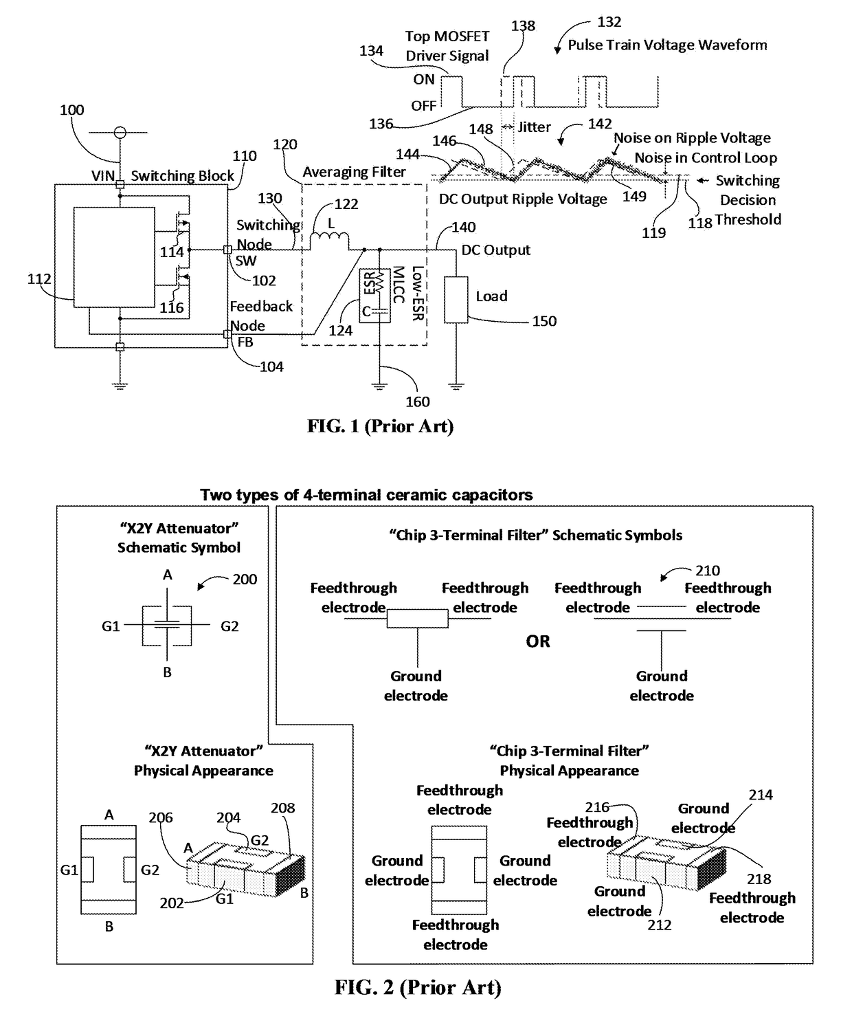
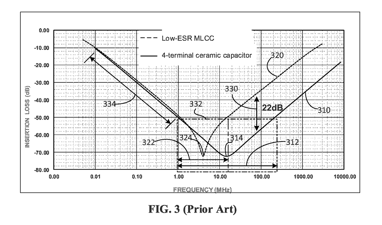
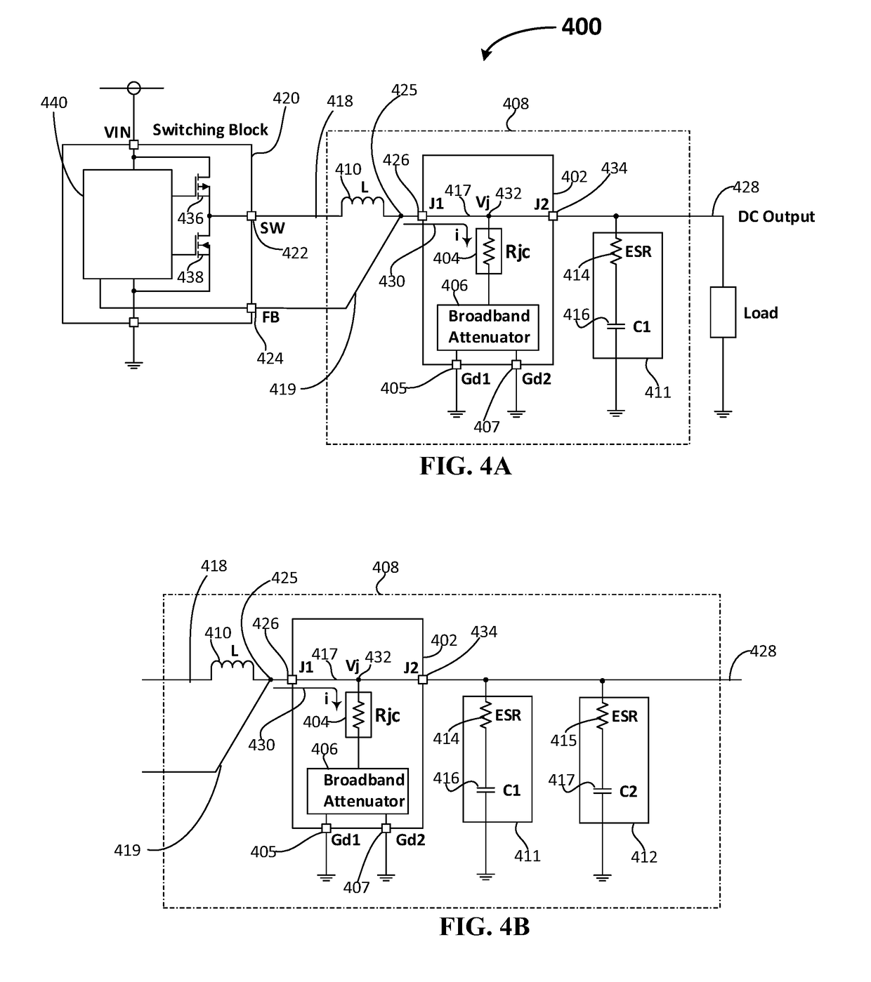
[0038]Construction of control circuits, averaging filters, and DC-DC converters using a passive signal conditioning device are described in the following description using specific language that has been briefly introduced in the previous section of BACKGROUND OF THE INVENTION and FIGS. 1, 2 and 3. Numerous specific details are set forth, such as circuit topology, circuit models, circuit functions, and circuit parameters, in order to provide a thorough understanding of embodiments of the present invention. Reference numbers may be repeated throughout the embodiments and Figures for properly indexing certain circuit parameters with respect to specific circuit elements. It will nevertheless be understood that the embodiments and examples are not intended to be limiting. Any alterations and modifications in the disclosed embodiments, and any further applications of principles disclosed in this document are contemplated as would normally occur to one of ordinary skill in the pertinent a...


PUM


Abstract

A circuit arrangement and methods for reducing a time domain noise signature (switching noise jitter (SNJ) signature) in output and feedback paths of a feedback control loop circuitry having a transistor switching stage switching an output signal at one or more predetermined frequencies are disclosed. In an example, the circuit arrangement has a feedback control loop circuitry including a first means, a common connection junction, one or more signal terminals, one or more rails and a passive signal conditioning means. The passive signal conditioning means including the rails is closely coupled to the common connection junction and is characterized by a set of specified characteristics to condition pre-existing noise amplitude and slopes of an analog signal having a plurality of noise carrying jittering ramps. The set of specified characteristics is configured to provide substantial attenuation to the pre-existing noise amplitude in specified low and high frequency bands and steepen the slopes of the noise carrying jittering ramps with the substantially attenuated noise amplitude of the analog signal so as to improve the interactions between the analog signal and the feedback control loop circuitry, thereby the SNJ signature, which is produced by transient noise displacement or noise perturbation in the time domain when the analog signal jitters, can be reduced in the output and feedback paths of the feedback control loop circuitry, notwithstanding the fact that the signal conditioned analog signal still jitters. In another example, the set of specified characteristics of the passive signal conditioning means includes a first substantial predetermined signal conditioning equivalent series resistance (ESR). In another example, the circuit arrangement further comprises a frequency domain filter part disposed farther than the passive signal conditioning means from the common connection junction, and a ratio of the first substantial predetermined signal conditioning ESR to the corresponding ESR of the frequency domain filter part is characterized to be substantially greater than 1. In another example, the passive signal conditioning means comprises a selected filter or capacitor denoted as X2Y, of which is characterized to satisfy the set of specified characteristics. In another example, the frequency domain filter part comprises at least three terminals.

Description

CROSS REFERENCE TO RELATED APPLICATIONS[0001]This application is a continuation of International Application Serial No. PCT / US2017 / 023268 filed on Mar. 21, 2017, which claims the benefit of priority under 35 USC § 119(e) to U.S. Provisional Patent Application No. 62 / 310,673 filed on Mar. 19, 2016, which are incorporated herein by reference in their entireties.BACKGROUND OF THE INVENTIONField of the Invention[0002]This invention provides a circuit arrangement for reducing a time domain noise signature (switching noise jitter (SNJ) signature) of control circuits that include negative feedback loops which may be applied to switching mode DC-DC converters, particularly those DC-DC converters that include pulse frequency modulation (PFM) types of conversion, thereby improving the performance of noise-sensitive circuits and electronics systems connected thereto, the SNJ signature being detrimental to the signal integrity of the noise-sensitive applications.Related Art[0003]DC-DC converter...

Claims


Application Information

Patent Timeline
Patent Type & Authority Applications(United States)
IPC IPC(8): G01R31/317H02M3/158H02M1/44H01P1/22
CPCG01R31/31709H02M3/158H02M1/44H01P1/227H02M3/156Y02B70/10H02M1/0054H02M1/143H03M1/0836
Inventor WONG, CHIH WEI
Owner TRANSSIP
Why Eureka
Try Eureka