Enhancement-mode gan-based HEMT device on si substrate and manufacturing method thereof

a technology of gan-based hemt and hemt substrate, which is applied in the field of microelectronics, can solve the problems of degradation and reliability problems in the electrical performance of gan-based high-voltage switching device, difficult for monocrystalline gan-based epitaxial material to grow flatly on the large-sized si substrate, and difficult to achieve cmos compatibility, suppress material failure, and improve film quality

Active Publication Date: 2019-04-11
SOUTH CHINA UNIV OF TECH
View PDF0 Cites 16 Cited by
  • Summary
  • Abstract
  • Description
  • Claims
  • Application Information

AI Technical Summary

Benefits of technology

[0039]The device is an enhancement-mode GaN-based HEMT device on a Si substrate that makes it easier to achieve CMOS-compatible GaN electronic device process. At the same time, the enhanced MIS-HEMT is prepared on the depletion-mode epitaxial material by using the mature ALD and LPCVD insulating film growth techniques in CMOS. By optimizing the process conditions, on the one hand, it suppresses material failure, and on the other hand, improves the film quality. At the same time, the interface state of the semiconductor / dielectric layer is improved; a high-quality insulating gate dielectric is fabricated; the surface state is reduced, and a large gate voltage level is achieved, therefore it has characteristics of high threshold voltage, high breakdown voltage and high current density, and has excellent pinch-off characteristic, as well as the characteristics of simple manufacturing process and good reproducibility, and is suitable for applications such as high voltage and high power electronic devices.

Problems solved by technology

Due to the large lattice mismatch (−17%) and thermal mismatch (116%) between GaN and Si substrates, it is very difficult for the monocrystalline GaN-based epitaxial material to grow flatly on the large-sized Si substrate.
This tensile stress due to thermal mismatch will cause the epitaxial wafer to be strongly warped or even cracked.
During the growth and the optimization of the GaN-based heterojunction structure on the large-sized Si substrate, the AlGaN barrier layer is subjected to the tensile stress applied by the GaN channel layer, and various defects are introduced by the release of stress into the heterojunction, thereby causing the degradation and reliability problems in the electrical performance of the GaN-based high voltage switching device.
The growth of the GaN-based heterojunction structure on the Si substrate is more difficult, since the GaN-based material on the Si substrate have higher defect densities (including dislocations and background impurities), and the GaN-based material is subjected to greater stress.
More defects and larger stress will urge the accelerated release of stress in the GaN-based heterojunction structure on the Si substrate, which causes reliability problems of the device.

Method used


Image

  • Enhancement-mode gan-based HEMT device on si substrate and manufacturing method thereof
  • Enhancement-mode gan-based HEMT device on si substrate and manufacturing method thereof
  • Enhancement-mode gan-based HEMT device on si substrate and manufacturing method thereof

Examples


Embodiment Construction

[0043]The specific implementation of the present invention is further described below with reference to the accompanying drawings and embodiment, but the implementation and protection of the present invention are not limited thereto. It should be noted that, if any process or process parameters are not described in detail below, it can be achieved with reference to the prior art by those skilled in the art.

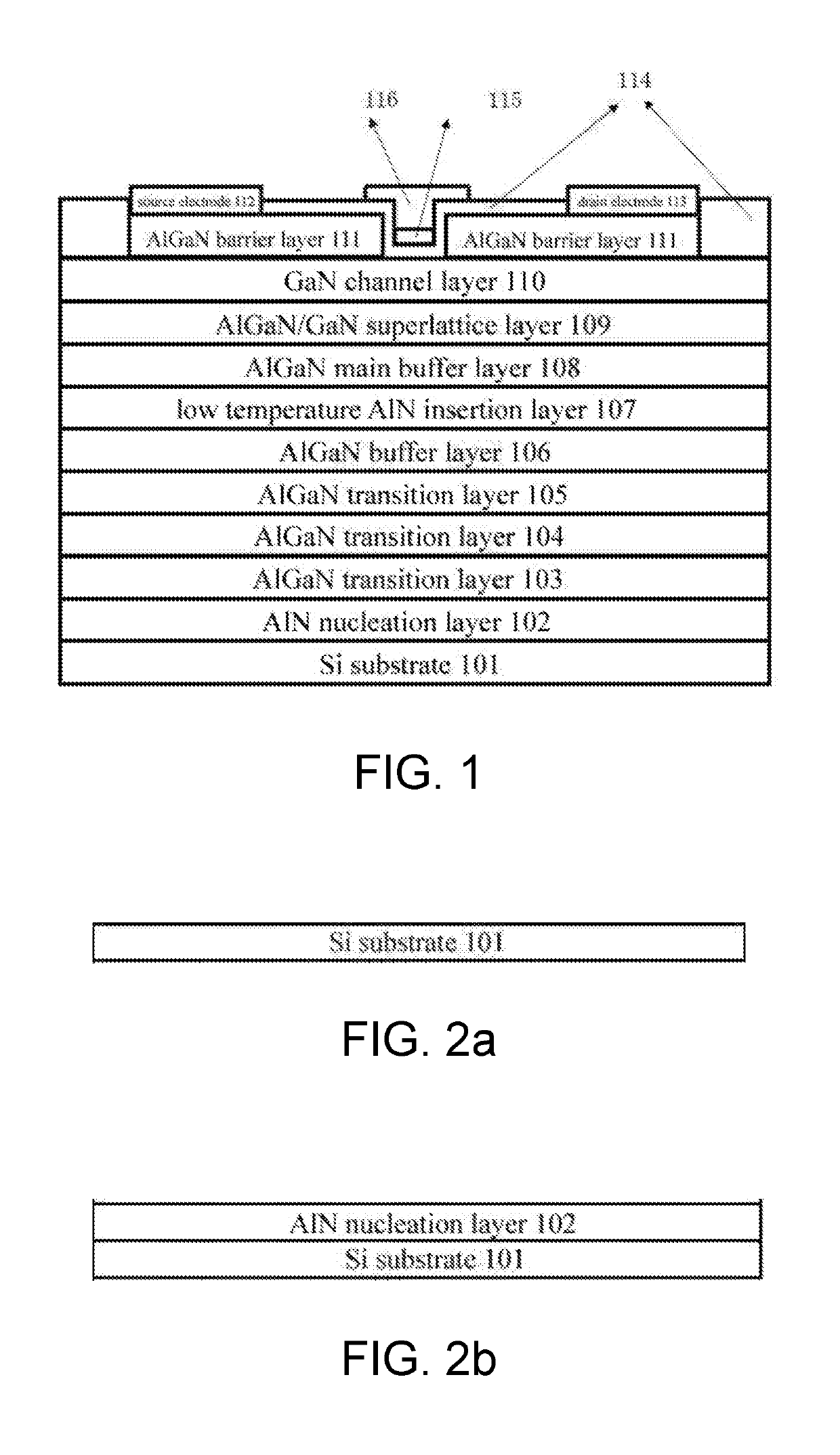
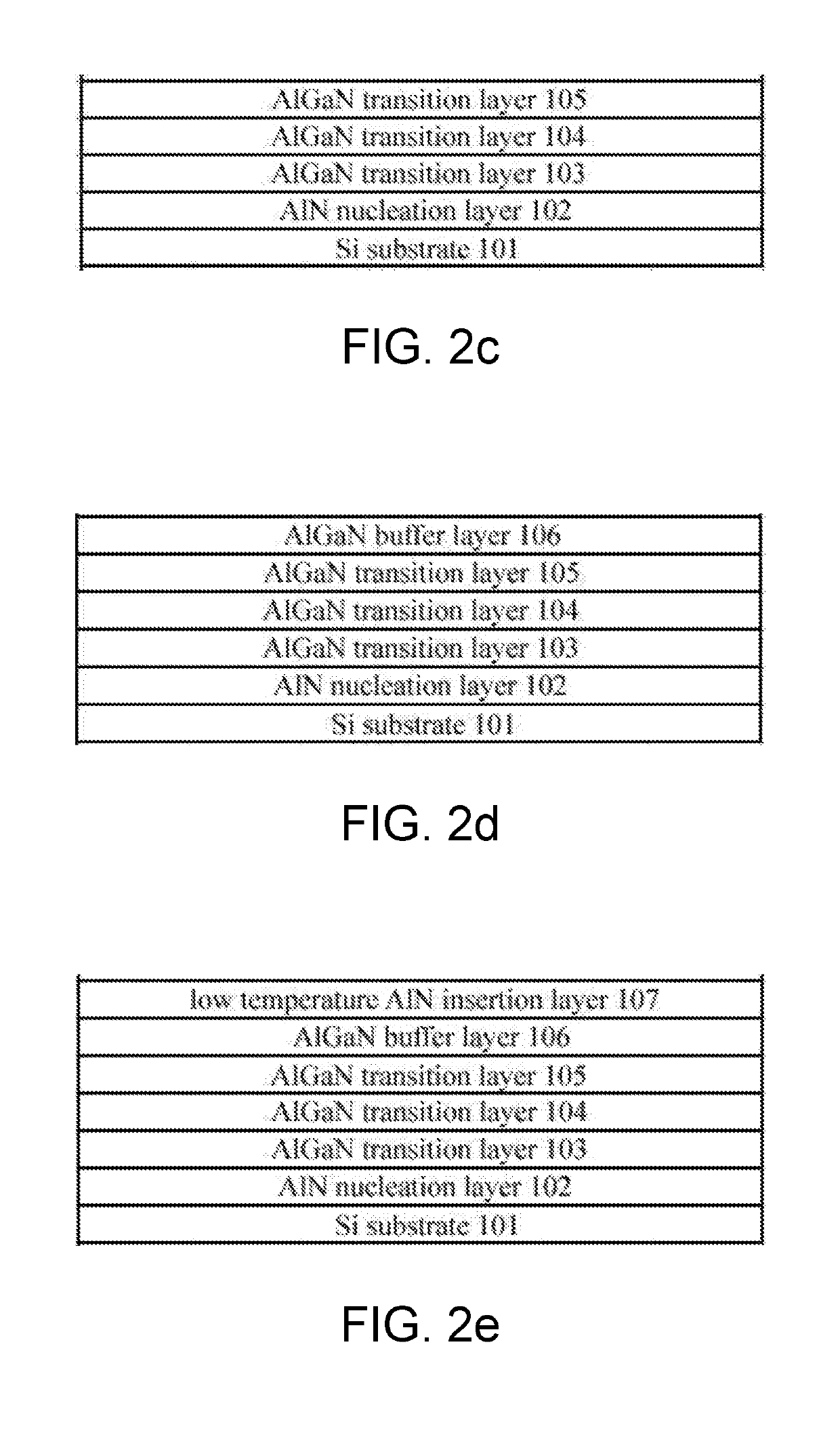
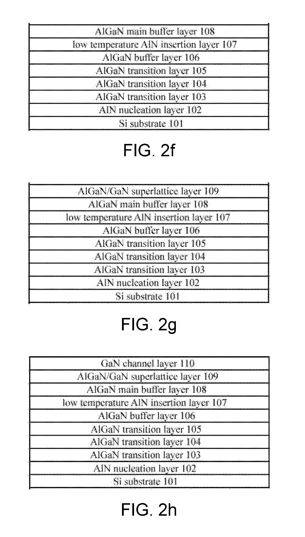
[0044]Referring to FIG. 1, an enhancement-mode GaN-based HEMT device on a Si substrate includes: a Si substrate 101, an AlN nucleation layer 102, AlGaN transition layers 103-105, an AlGaN buffer layer 106, a low temperature AlN insertion layer 107, an AlGaN main buffer layer 108, a AlGaN / GaN superlattice layer 109, a GaN channel layer 110, and a AlGaN barrier layer 111. Both sides of a top end of the HEMT device are a source electrode 112 and a drain electrode 113 respectively, and a middle of the top end is a gate electrode 116. A passivation protective layer 114 is deposited on ...


PUM

PropertyMeasurementUnit
sizeaaaaaaaaaa
thicknessesaaaaaaaaaa
temperatureaaaaaaaaaa

Abstract

An enhancement-mode GaN-based HEMT device on Si substrate and a manufacturing method thereof. The device includes a Si substrate, an AlN nucleation layer, AlGaN transition layers, an AlGaN buffer layer, a low temperature AlN insertion layer, an AlGaN main buffer layer, an AlGaN/GaN superlattice layer, an GaN channel layer), and an AlGaN barrier layer. Both sides of a top end of the HEMT device are a source electrode and a drain electrode respectively, and a middle of the top end is a gate electrode. A middle of the AlGaN barrier layer is etched through to form a recess, and a bottom of the recess is connected to the GaN channel layer. A passivation protective layer and a gate dielectric layer are deposited on the bottom of the recess, and the gate electrode is located above the dielectric layer.

Description

BACKGROUNDTechnical Field[0001]The present invention belongs to the technical field of microelectronics and relates to semiconductor devices, in particular to an enhancement-mode GaN-based HEMT device on Si substrate and a manufacturing method thereof, which can be used in a high voltage and high power application and constitute a basic unit of a digital circuit.Description of Related Art[0002]With the development of modern weaponry and aerospace, nuclear power, communication technology, automotive electronics, and switching power supplies, higher requirements are placed on the performance of semiconductor devices. As a typical representative of wide-bandgap semiconductor materials, GaN-based material has the characteristics such large width of bandgap, high electron saturation drift velocity, high critical breakdown field strength, high thermal conductivity, good stability, corrosion resistance, radiation resistance and so on. In addition, GaN also has excellent electronic properti...

Claims


Application Information

Patent Timeline
Patent Type & Authority Applications(United States)
IPC IPC(8): H01L29/66H01L29/20H01L29/778H01L29/205H01L21/02
CPCH01L29/66431H01L29/2003H01L29/778H01L29/205H01L21/02381H01L21/02458H01L21/02507H01L21/0254H01L21/02505H01L29/4236H01L29/66462H01L29/7786
Inventor WANG, HONGZHOU, QUANBINLI, QIXIN
Owner SOUTH CHINA UNIV OF TECH
Why Eureka
Try Eureka