OLED touch display panel and driving method thereof

a technology of touch display panel and driving method, which is applied in the direction of electric digital data processing, instruments, computing, etc., can solve the problems of increasing manufacturing cost, reducing yield rate, and complex structures and manufacturing processes, and achieve accurate identification

Active Publication Date: 2019-05-09
WUHAN CHINA STAR OPTOELECTRONICS SEMICON DISPLAY TECH CO LTD
View PDF4 Cites 2 Cited by
  • Summary
  • Abstract
  • Description
  • Claims
  • Application Information

AI Technical Summary

Benefits of technology

[0047]Beneficial effects of the present disclosure are: compared to existing technology, the present disclosure, by dividing the cathode layer into the two sub-cathodes separated from each other and also serving as touch electrodes, by connecting the touch electrodes to the touch chip through the touch signal lines, and by time-division driving the OLED touch display panel using the array circuit layer, accurate positioning of touched positions may be realized, and meanwhile, thickness of a module may be decreased.

Problems solved by technology

Currently, people increasingly demand displaying fineness, i.e., resolution, but there exists many challenges in producing high quality and high resolution OLED displays.
Therefore, both structures and manufacturing processes are more complicated.
Increased manufacturing process difficulty causes adverse effects, such as decreased yield rates, increasing manufacturing cost.
Hence, a distance between the cathode layer and an upper touch electrode layer is very short, resulting in noise interference coming from OLEDs being huge, and parasitic capacitance between touch electrodes and cathodes being large, causing variation amounts of self-mutual capacitance to be too small after the existing OLED touch display panel is touched, and touched positions to be unable to be accurately identified.

Method used


Image

  • OLED touch display panel and driving method thereof
  • OLED touch display panel and driving method thereof
  • OLED touch display panel and driving method thereof

Examples


first embodiment

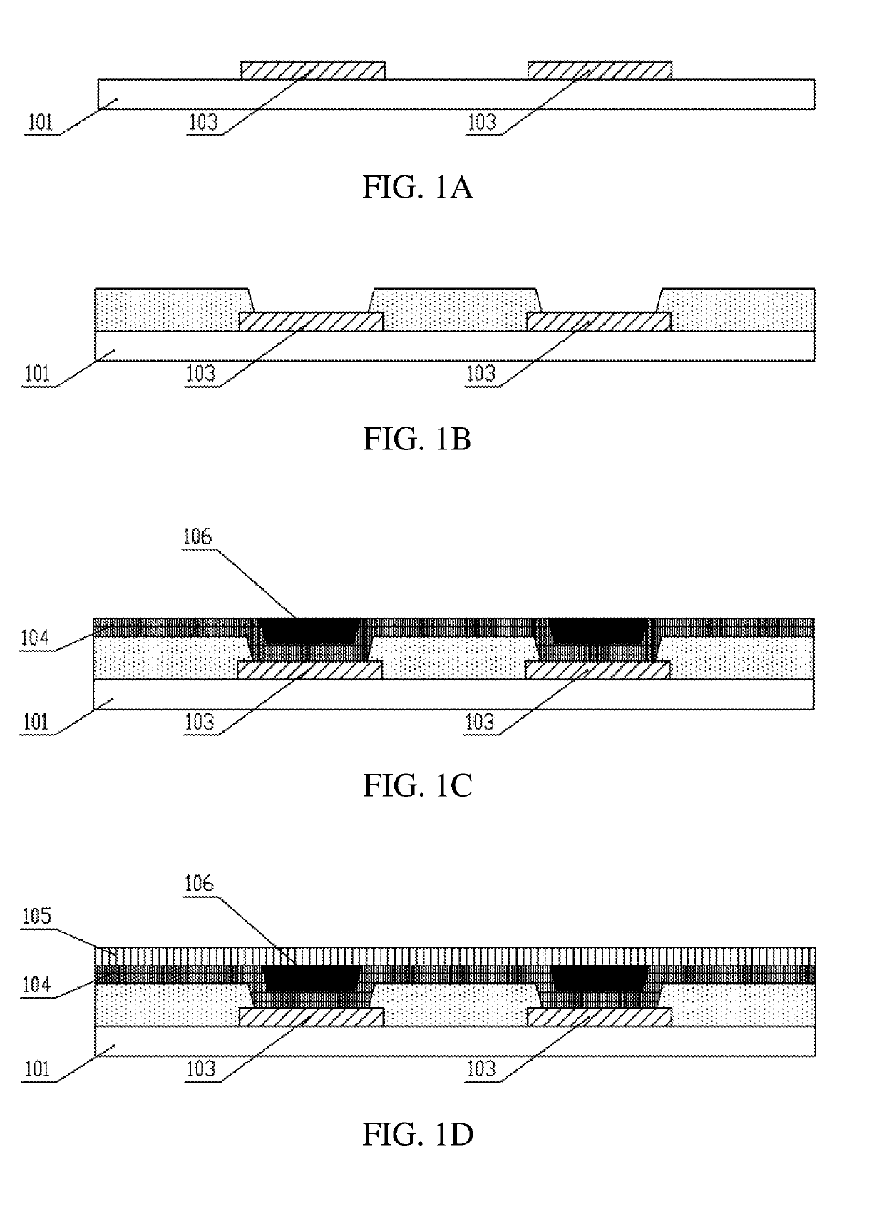
[0059]First, a glass substrate is provided, and an array circuit layer is deposited over the glass substrate, to form a base substrate 101. The array circuit layer includes a buffer layer, an active layer, a gate-insulating layer, a gate electrode layer, an inter-insulating layer, a source drain electrode layer, and a passivation layer.

[0060]In the present embodiment, preferably, the active layer is a metal oxide thin film, such as indium gallium zinc oxide, and the oxide is a semiconductor. Material of the gate-insulating layer is usually silicon nitride, or may also be material such as silicon oxide or silicon oxynitride. The gate electrode layer and the source drain electrode layer may be made of metal such as molybdenum, aluminum, aluminum-nickel alloy, molybdenum-tungsten alloy, chromium, or copper, or a combined structure of thin films of the aforementioned materials. The passivation layer 214 is usually a silicon nitride compound.

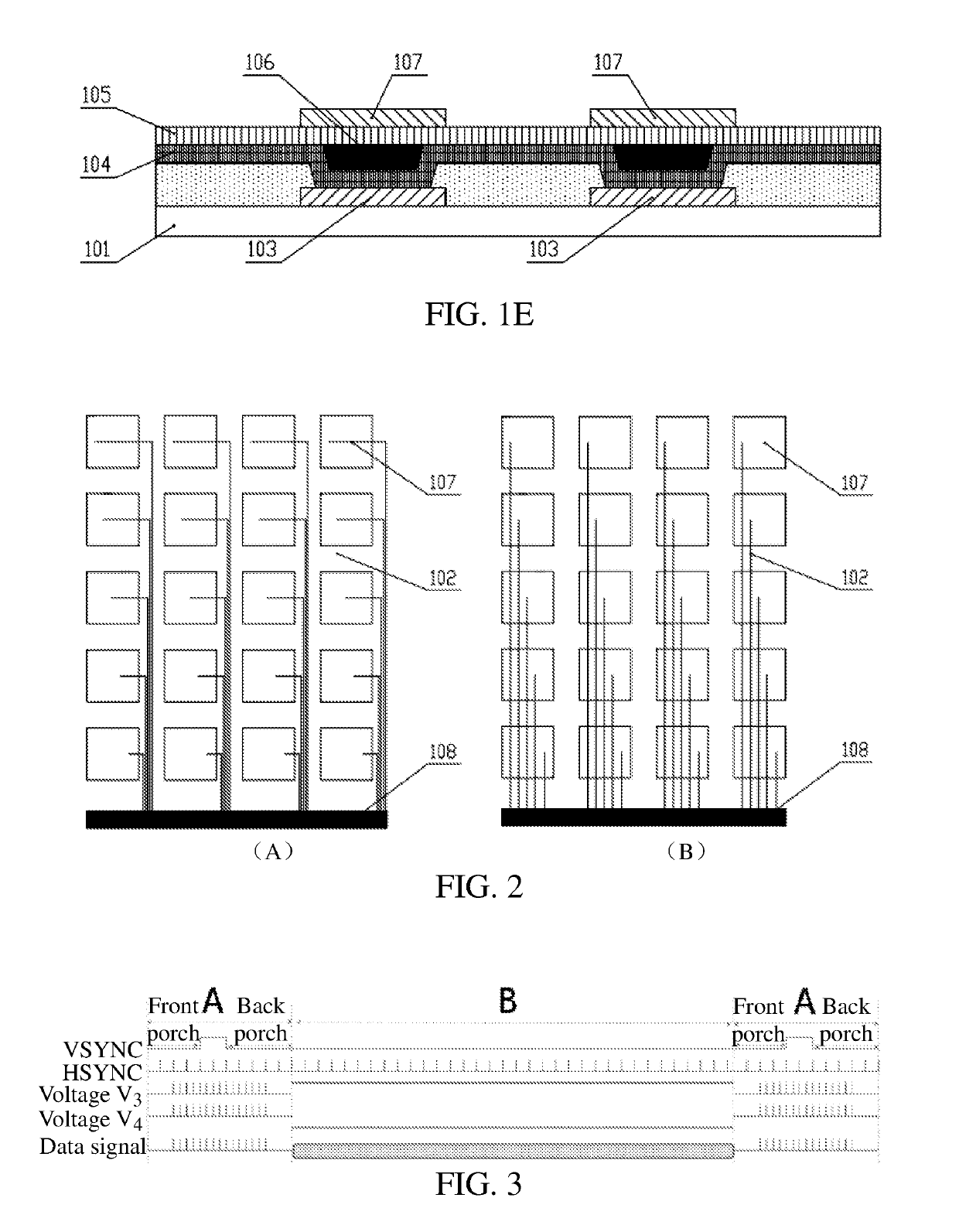
[0061]As illustrated in FIG. 1A, an anode laye...

second embodiment

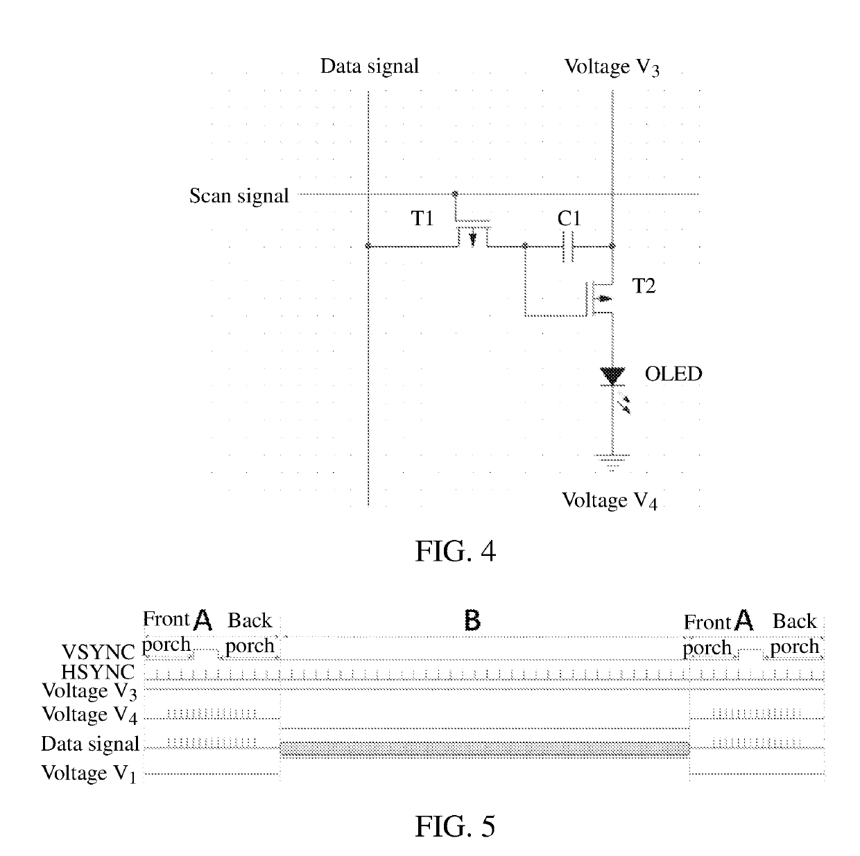
[0081]FIG. 5 is a circuit timing diagram of an OLED touch display panel in accordance with a second preferred embodiment of the present disclosure. The circuit timing diagram includes a display stage and a touch control stage. The touch control stage is denoted using “A”, and the display stage is denoted using “B”. FIG. 6 is a pixel circuit diagram of an OLED touch display panel in accordance with a second preferred embodiment of the present disclosure. In the present embodiment, preferably, T1 is a P-type thin film transistor, T2 is an N-type thin film transistor, T3 is a P-type thin film transistor, a voltage V2 is an enable signal voltage, a voltage V3 is a voltage ELVDD, i.e., an OLED anode voltage, and a voltage V4 is a voltage ELVSS, i.e., an OLED cathode voltage.

[0082]During the display period, similar to the first embodiment, in a pixel circuit of the OLED touch display panel, a low-level voltage at the first input terminal turns on the thin film transistor T1, a high-level ...


PUM


Abstract

An OLED touch display panel and a driving method are provided. The OLED touch display panel includes a cathode layer. The cathode layer is divided into the two sub-cathodes separated from each other and also serving as touch electrodes. In a pixel circuit of the OLED touch display panel, under common operations of a first input terminal and a second input terminal fed with different voltages, the OLED touch display panel normally emits light or does not emit light.

Description

FIELD OF INVENTION[0001]The present disclosure relates to a technical field of flat panel display manufacturing, and more particularly to an organic light-emitting diode (OLED) touch display panel and a driving method thereof.BACKGROUND OF INVENTION[0002]In flat panel display technology, organic light-emitting diode (OLED) displays have the advantages of being lightweight and slim, and having active light emission, fast response speed, large viewing angles, wide color gamuts, high brightness, low power consumption, etc., and have gradually become third generation display technology after liquid crystal displays. Compared to liquid crystal displays (LCDs), OLEDs have the advantages of being more power saving and slimmer, and having wide viewing angles, which are unmatched by LCDs. Currently, people increasingly demand displaying fineness, i.e., resolution, but there exists many challenges in producing high quality and high resolution OLED displays.[0003]With the development of portab...

Claims


Application Information

Patent Timeline
Patent Type & Authority Applications(United States)
IPC IPC(8): G06F3/041G09G3/3258G06F3/044
CPCG06F3/0418G09G3/3258G06F3/0412G06F3/044G09G2300/0426G06F3/0443G06F3/04164G06F3/04184G09G3/3233G09G2300/0842G09G2310/0251G09G2354/00H10K59/40
Inventor LIN, DANLIU, MINLUNDAI, QIBING
Owner WUHAN CHINA STAR OPTOELECTRONICS SEMICON DISPLAY TECH CO LTD
Why Eureka
Try Eureka